CY25568
Spread Spectrum Clock Generator
Cypress Semiconductor Corporation
http://www.cypress.com
Document#: 38-07111 Rev. *A
06/21/01
Page 7 of 12
Approved Product
S0, S1, D0, D1 and FRSEL digital inputs of the CY25568 are designed to sense 3 different logic levels designated
as High “1”, Low “0” and Middle “M”. With this 3-Level digital input logic, the CY25568 is able to detect 9 different
logic states in the case of (S0, S1) and (D0, D1) logic pairs and 3 different logic states in the case of FRSEL.
S0, S1, D0, D1 and FRSEL pins include an on chip 20K (10K /10K) resistor divider. No external application
resistors are needed to implement the 3-Level logic levels as shown below:
Logic State “0” = 3-Level logic pin connected to GND.
Logic State “M” = 3-Level logic pin left floating (no connection).
Logic State “1” = 3-Level logic pin connected to VDD.
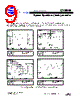
Figure 3 illustrates how to implement 3-Level Logic.
POWER DOWN (PD#)
CY25568 includes a Power Down (PD#, Pin 10) function. This input uses standard 2-Level CMOS logic and is
internally pulled up to VDD (HIGH). Connect this pin to GND if power is to be turned off.
MODULATION RATE
Spread Spectrum Clock Generators utilize frequency modulation (FM) to distribute energy over a specific band of
frequencies. The maximum frequency of the clock (fmax) and minimum frequency of the clock (fmin) determine
this band of frequencies. The time required to transition from fmin to fmax and back to fmin is the period of the
Modulation Rate, Tmod. The Modulation Rate of SSCG clocks are generally referred to in terms of frequency or
fmod = 1/Tmod.
The input clock frequency, fin, and the internal divider determine the Modulation Rate.
In the case of CY25568, the (Spread Spectrum) Modulation Rate is given by the following formula: fmod = fin/DR
Where; fmod is the Modulation Rate, fin is the Input Frequency and DR is the Divider Ratio as given in Table 8.
Notice that Input Frequency Range is set by FRSEL.
FRSEL
INPUT FREQUENCY
RANGE (MHz)
DIVIDER RATIO
(DR)
0
4 to 8
128
1
8 to 16
256
M
16 to 32
512
Table 8

 British ▼
 English
 Chinese
 German
 Japanese
 Russian
 Korean
 Spanish
 French
 Italian
 Portuguese
 Polish
 Vietnamese
 Indian
 Mexican
 British
 New Zealand