|
Electronic Components Datasheet Search |
|
|
Electronic Components Datasheet Search |
|
MAX1434EVKIT Datasheet(PDF) 7 Page - Maxim Integrated Products |
|
|
|||||||||||||||||||||||||||||
MAX1434EVKIT Datasheet(HTML) 7 Page - Maxim Integrated Products |
|
|
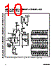
7 / 23 page  Double-Termination Settings The ADC features trimmed, internal 100 Ω termination resistors between the positive (true) and negative (complementary) line of each output (D0–D7, CLKOUT, and FRAME). The EV kit circuit also features 100 Ω ter- mination resistors located at the far end of each differ- ential output pair. Activating the internal termination helps eliminate unwanted reflections on the signal traces. Use jumper JU1 to activate either single or dou- ble-termination. See Table 8 for appropriate shunt posi- tions that select the termination architecture. SLVS/LVDS Outputs The ADC is capable of generating SLVS or LVDS signals at its outputs. Jumper JU2 controls this feature of the ADC. See Table 9 for shunt positions. Regardless of which output signal type is selected, the output buffers (U7–U16) will convert the data to LVPECL logic levels. When operating in SLVS output mode, JU1 must be con- figured for double-termination (shunt across pins 1 and 2). LVDS Test Pattern To debug signal integrity problems, the ADC can gen- erate a factory-set test pattern on all of the output chan- nels. Jumper JU3 controls this feature. See Table 10 for the appropriate shunt positions. The test pattern for the MAX1436, MAX1437, and MAX1438 is 0000 1011 1101. The test pattern for the MAX1434 is 00 0101 1101 (MSB to LSB). Output Bit Locations The digital outputs of the ADC are connected to the 40- pin header J9. All PC board trace lengths are matched to minimize data skew and improve the overall dynamic performance of the device. Additionally, 10 drivers (U7–U16) buffer and level-translate the digital outputs to LVPECL-compatible signals. The drivers increase the differential voltage swing, and are capable of driving large capacitive loads, which may be present at the logic analyzer connection. The outputs of the buffers are connected with 40-pin header J15. See Table 11 for bit locations of headers J9 and J15. MAX1434/MAX1436/MAX1437/MAX1438 Evaluation Kits _______________________________________________________________________________________ 7 SHUNT POSITION DT PIN CONNECTION EV KIT FUNCTION 1-2 AVDD Double Termination Selected. Outputs are double-terminated. 2-3* GND Single Termination Selected. Outputs are single-terminated. Table 8. Double-Termination Jumper Settings (JU1) * Default configuration: JU1 (2-3). SHUNT POSITION SLVS/ LVDS PIN CONNECTION ADC OUTPUT 1-2 AVDD SLVS 2-3* GND LVDS Table 9. SLVS/ LVDS Jumper Settings (JU7) * Default configuration: JU7 (2-3). SHUNT POSITION LVDSTEST PIN CONNECTION EV KIT FUNCTION 1-2 AVDD Test pattern transmitted, LSB first, on all SLVS/LVDS outputs 2-3* GND Normal operation Table 10. LVDS Test Pattern Jumper Settings (JU3) * Default configuration: JU3 (2-3). SIGNAL UNBUFFERED (LVDS or SLVS) BUFFERED (LVPECL) DESCRIPTION P J9-1 J15-1 CH0 N J9-2 J15-2 Channel 0 P J9-5 J15-5 CH1 N J9-6 J15-6 Channel 1 P J9-9 J15-9 CH2 N J9-10 J15-10 Channel 2 P J9-13 J15-13 CH3 N J9-14 J15-14 Channel 3 P J9-17 J15-17 CLKOUT N J9-18 J15-18 Clock P J9-21 J15-21 FRAME N J9-22 J15-22 Frame P J9-25 J15-25 CH4 N J9-26 J15-26 Channel 4 P J9-29 J15-29 CH5 N J9-30 J15-30 Channel 5 P J9-33 J15-33 CH6 N J9-34 J15-34 Channel 6 P J9-37 J15-37 CH7 N J9-38 J15-38 Channel 7 Table 11. Output Bit Locations P = True (+). N = Complementary (-). |
|
|
Link URL |
| Does ALLDATASHEET help your business so far? [ DONATE ] |
About Alldatasheet | Advertisement | Contact us | Privacy Policy | Link to Datasheet | Link Exchange | Manufacturer List All Rights Reserved©Alldatasheet.com |
| Russian : Alldatasheetru.com | Korean : Alldatasheet.co.kr | Spanish : Alldatasheet.es | French : Alldatasheet.fr | Italian : Alldatasheetit.com Portuguese : Alldatasheetpt.com | Polish : Alldatasheet.pl | Vietnamese : Alldatasheet.vn Indian : Alldatasheet.in | Mexican : Alldatasheet.com.mx | British : Alldatasheet.co.uk | New Zealand : Alldatasheet.co.nz |
|
Family Site : ic2ic.com |
icmetro.com |
 British ▼
 English
 Chinese
 German
 Japanese
 Russian
 Korean
 Spanish
 French
 Italian
 Portuguese
 Polish
 Vietnamese
 Indian
 Mexican
 British
 New Zealand