|
Electronic Components Datasheet Search |
|
|
Electronic Components Datasheet Search |
|
ADP5076ACBZ-R7 Datasheet(PDF) 14 Page - Analog Devices |
|
|
|||||||||||||||||||||||||||||
ADP5076ACBZ-R7 Datasheet(HTML) 14 Page - Analog Devices |
|
|
14 / 23 page 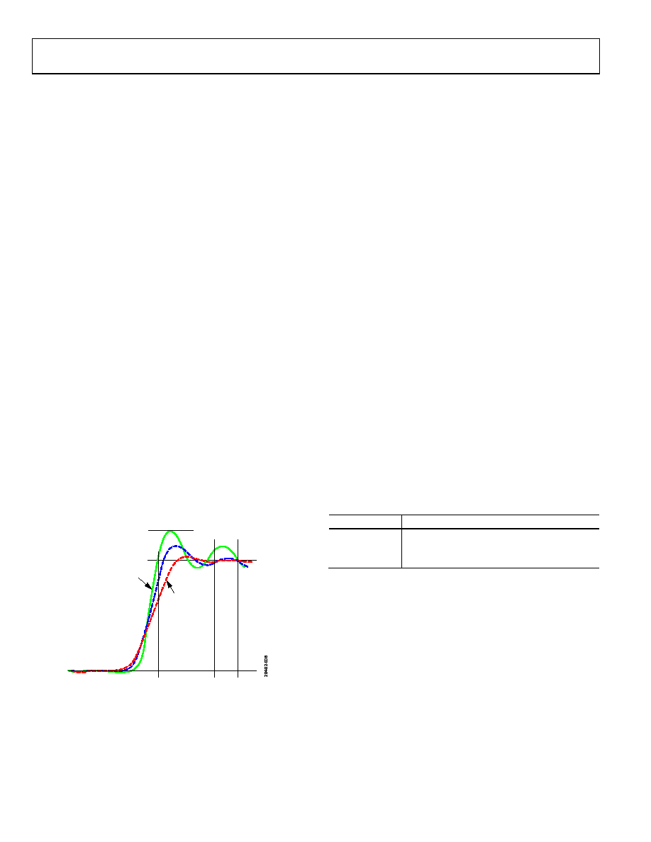 ADP5076 Data Sheet Rev. A | Page 14 of 23 PRECISION ENABLING The ADP5076 has an individual enable pin for the boost regulator (EN1) and inverting regulator (EN2). These enable pins feature a precision enable circuit with an accurate reference voltage. This reference allows the ADP5076 to be sequenced easily from other supplies. It can also be used as a programmable UVLO input by using a resistor divider. The enable pins have an internal pull-down resistor that defaults each regulator to off when the pin is floating. When the voltage of the enable pins is greater than the VTH_H reference level, the regulator is enabled. SOFT START Each regulator in the ADP5076 includes soft start circuitry that ramps the output voltage in a controlled manner during startup, limiting the inrush current. The soft start time is internally set to the fastest rate when the SS pin is open. Connecting a resistor between the SS pin and the AGND pin allows the adjustment of the soft start delay. The delay length is common to both regulators. SLEW RATE CONTROL The ADP5076 employs programmable output driver slew rate control circuitry. This circuitry reduces the slew rate of the switching node as shown in Figure 40, resulting in reduced ringing and lower EMI. To program the slew rate, connect the SLEW pin to the AVIN pin for normal mode, to the AGND pin for slow mode, or leave it open for fast mode. This configuration allows the use of an open-drain output from a noise sensitive device to switch the slew rate from fast to slow, for example, during ADC sampling. Slew rate control causes a trade-off between efficiency and low EMI. FASTEST SLOWEST Figure 40. Switching Node at Various Slew Rate Settings CURRENT-LIMIT PROTECTION The boost and inverting regulators in the ADP5076 include current-limit protection circuitry to limit the amount of forward current through the MOSFET switch. When the peak inductor current exceeds the overcurrent limit threshold for a number of clock cycles during an overload or short-circuit condition, the regulator enters hiccup mode. The regulator stops switching and then restarts with a new soft start cycle after tHICCUP and repeats until the overcurrent condition is removed. OVERVOLTAGE PROTECTION An overvoltage protection mechanism is present on the FB1 and FB2 pins for the boost and inverting regulators. On the boost regulator, when the voltage on the FB1 pin exceeds the VOV1 threshold, the switching on SW1 stops until the voltage falls below the threshold again. This functionality is permanently enabled on this regulator. On the inverting regulator, when the voltage on the FB2 pin drops below the VOV2 threshold, the switching stops until the voltage rises above the threshold. This functionality is enabled after the soft start period has elapsed. THERMAL SHUTDOWN In the event that the ADP5076 junction temperature rises above TSHDN, the thermal shutdown circuit turns off the integrated circuit (IC). Extreme junction temperatures can be the result of prolonged high current operation, poor circuit board design, and/or high ambient temperature. Hysteresis is included so that when thermal shutdown occurs, the ADP5076 does not return to operation until the on-chip temperature drops below TSHDN − THYS. When resuming from thermal shutdown, a soft start is performed on each enabled channel. STARTUP SEQUENCE The ADP5076 implements a flexible startup sequence to meet different system requirements. Three different enabling modes can be implemented via the SEQ pin, as explained in Table 7. Table 7. SEQ Pin Settings SEQ Pin Description Open Manual enable mode AVIN Simultaneous enable mode Low Sequential enable mode To configure the manual enable mode, leave the SEQ pin open. The boost and inverting regulators are controlled separately from their respective precision enable pins. To configure the simultaneous enable mode, connect the SEQ pin to the AVIN pin. Both regulators power up simultaneously when the EN2 pin is taken high. The EN1 pin enable can be used to enable the internal references ahead of enabling the outputs, if desired. The simultaneous enable mode timing is shown in Figure 41. |
|
|
Link URL |
| Does ALLDATASHEET help your business so far? [ DONATE ] |
About Alldatasheet | Advertisement | Contact us | Privacy Policy | Link to Datasheet | Link Exchange | Manufacturer List All Rights Reserved©Alldatasheet.com |
| Russian : Alldatasheetru.com | Korean : Alldatasheet.co.kr | Spanish : Alldatasheet.es | French : Alldatasheet.fr | Italian : Alldatasheetit.com Portuguese : Alldatasheetpt.com | Polish : Alldatasheet.pl | Vietnamese : Alldatasheet.vn Indian : Alldatasheet.in | Mexican : Alldatasheet.com.mx | British : Alldatasheet.co.uk | New Zealand : Alldatasheet.co.nz |
|
Family Site : ic2ic.com |
icmetro.com |
 British ▼
 English
 Chinese
 German
 Japanese
 Russian
 Korean
 Spanish
 French
 Italian
 Portuguese
 Polish
 Vietnamese
 Indian
 Mexican
 British
 New Zealand