|
Electronic Components Datasheet Search |
|
|
Electronic Components Datasheet Search |
|
ADP5076ACBZ-R7 Datasheet(PDF) 19 Page - Analog Devices |
|
|
|||||||||||||||||||||||||||||
ADP5076ACBZ-R7 Datasheet(HTML) 19 Page - Analog Devices |
|
|
19 / 23 page 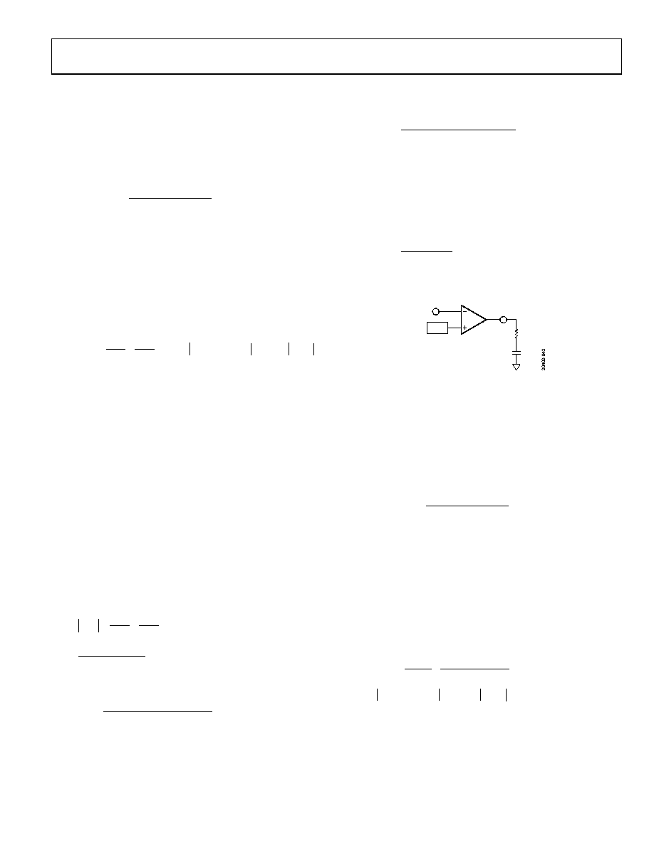 Data Sheet ADP5076 Rev. A | Page 19 of 23 Boost Regulator The boost converter produces an undesirable right half plane zero in the regulation feedback loop. This feedback loop requires compensating the regulator so that the crossover frequency is less than the frequency of the right half plane zero. The right half plane zero frequency is determined by the following equation: 2 (1 ) () 2 1 LOAD1 Z1 R DUTY fRHP L1 where: fZ1(RHP) is the right half plane zero frequency. RLOAD1 is the equivalent resistor load for boost regulator, which is also equal to the output voltage divided by the load current. To stabilize the regulator, ensure that the regulator crossover frequency is less than or equal to one-tenth of the right half plane zero frequency. The boost regulator loop gain is FB1 IN VL1 M1 OUT1 COMP1 CS1 OUT1 POS POS VV AG R ||Z G Z VV where: AVL1 is the loop gain. VFB1 is the feedback regulation voltage. VPOS is the regulated positive output voltage. VIN is the input voltage. GM1 is the error amplifier transconductance gain. ROUT1 is the output impedance of the error amplifier and is 33 MΩ. ZCOMP1 is the impedance of the series RC network from the COMP1 pin to the AGND pin. GCS1 is the current sense transconductance gain (the inductor current divided by the voltage at the COMP1 pin), which is internally set by the ADP5076 and is 12.5 A/V. ZOUT1 is the impedance of the load in parallel with the output capacitor. At crossover frequency (fC1), the ZCOMP1 is dominated by a resistor (RC1), and the ZOUT1 is dominated by the impedance of an output capacitor (COUT1). Therefore, when solving for the fC1, the equation (by definition of the crossover frequency) is simplified to 1 2 1 OUT1 C1 CS1 C1 M1 POS IN POS FB1 VL1 C f π G R G V V V V A To solve for RC1, use the following equation: 2 2) C1 OUT1 POS C1 FB1 IN M1 CS1 fC (V R VV G G where GCS1 = 12.5 A/V. Using typical values for VFB1 and GM1 (see the Specifications section) results in 2 2094 ) C1 OUT1 POS C1 IN fC (V R V For better accuracy, it is recommended to use the COUT1 value expected under the dc bias conditions that the COUT1 value operates under in the calculation for RC1. After the compensation resistor is known, set the zero formed by the compensation capacitor and resistor to one-fourth of the crossover frequency, or 2 C1 C1 C1 C π fR where CC1 is the compensation capacitor value. ERROR AMPLIFIER REF1 gM1 FB1 COMP1 RC1 CC1 Figure 44. Compensation Components Inverting Regulator The inverting converter, like the boost converter, produces an undesirable right half plane zero in the regulation feedback loop. This feedback loop requires compensating the regulator so that the crossover frequency is less than the frequency of the right half plane zero. The right half plane zero frequency is determined by the following equation: (1 ) 2 2 2 LOAD2 Z2 2 R DUTY f (RHP) π L2 DUTY where: fZ2(RHP) is the right half plane zero frequency. RLOAD2 is the equivalent resistor load for inverting regulator, which is also equal to the output voltage divided by the load current. To stabilize the regulator, ensure that the regulator crossover frequency is less than or equal to one-tenth of the right half plane zero frequency. The inverting regulator loop gain is (2 | |) FB2 IN VL2 M2 NEG IN NEG OUT2 COMP2 CS2 OUT2 VV AG |V | V V R||Z G Z where: AVL2 is the loop gain. VFB2 is the FB2 reference voltage. VNEG is the regulated negative output voltage. VIN is the input voltage. GM2 is the error amplifier transconductance gain. ROUT2 is the output impedance of the error amplifier and is 33 MΩ. |
|
|
Link URL |
| Does ALLDATASHEET help your business so far? [ DONATE ] |
About Alldatasheet | Advertisement | Contact us | Privacy Policy | Link to Datasheet | Link Exchange | Manufacturer List All Rights Reserved©Alldatasheet.com |
| Russian : Alldatasheetru.com | Korean : Alldatasheet.co.kr | Spanish : Alldatasheet.es | French : Alldatasheet.fr | Italian : Alldatasheetit.com Portuguese : Alldatasheetpt.com | Polish : Alldatasheet.pl | Vietnamese : Alldatasheet.vn Indian : Alldatasheet.in | Mexican : Alldatasheet.com.mx | British : Alldatasheet.co.uk | New Zealand : Alldatasheet.co.nz |
|
Family Site : ic2ic.com |
icmetro.com |
 British ▼
 English
 Chinese
 German
 Japanese
 Russian
 Korean
 Spanish
 French
 Italian
 Portuguese
 Polish
 Vietnamese
 Indian
 Mexican
 British
 New Zealand