|
Electronic Components Datasheet Search |
|
|
Electronic Components Datasheet Search |
|
SI5350C-B Datasheet(PDF) 7 Page - Skyworks Solutions Inc. |
|
|
|||||||||||||||||||||||||||||
SI5350C-B Datasheet(HTML) 7 Page - Skyworks Solutions Inc. |
|
|
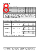
7 / 40 page  Si5350C-B Skyworks Solutions, Inc. • Phone [781] 376-3000 • Fax [781] 376-3100 • sales@skyworksinc.com • www.skyworksinc.com 7 Rev. 1.2 • Skyworks Proprietary Information • Products and Product Information are Subject to Change Without Notice • August 22, 2021 Table 7. Output Characteristics VDD = 1.8 V ±5%, 2.5 V ±10%, or 3.3 V ±10%, TA = –40 to 85 °C) Parameter Symbol Test Condition Min Typ Max Units Frequency Range1 FCLK 0.0025 — 200 MHz Load Capacitance CL FCLK < 100 MHz — — 15 pF Duty Cycle DC FCLK < 160 MHz, Measured at VDD/2 45 50 55 % FCLK > 160 MHz, Measured at VDD/2 40 50 60 % Rise/Fall Time tr/tf 20%–80%, CL = 5 pF — 1 1.5 ns Output High Voltage VOH CL =5pF VDD – 0.6 — — V Output Low Voltage VOL —— 0.6 V Period Jitter2,3 JPER 16, 20-QFN, 4 outputs run- ning, 1 per VDDO -40 95 ps, pk-pk 10-MSOP or 20-QFN, all outputs running - 70 155 ps, pk-pk Cycle-to-cycle Jitter2,3 JCC 16, 20-QFN, 4 outputs run- ning, 1 per VDDO —50 90 ps, pk 10-MSOP or 20-QFN, all outputs running — 70 150 ps, pk Notes: 1. Only two unique frequencies above 112.5 MHz can be simultaneously output. 2. Measured over 10k cycles. Jitter is only specified at the default high drive strength (50 output impedance). 3. Jitter is highly dependent on device frequency configuration. Specifications represent a “worst case, real world” frequency plan; actual performance may be substantially better. Three-output 10MSOP package measured with clock outputs of 74.25, 24.576, and 48 MHz. Eight-output 20QFN package measured with clock outputs of 33.33, 74.25, 27, 24.576, 22.5792, 28.322, 125, and 48 MHz. Four-output, 16-QFN package measured with clock outputs of 33.333, 27, 28.322, and 48 MHz. Table 8. 25 MHz Crystal Requirements1,2 Parameter Symbol Min Typ Max Unit Crystal Frequency fXTAL —25— MHz Load Capacitance CL 6— 12 pF Equivalent Series Resistance rESR —— 150 Crystal Max Drive Level dL 100 — — µW Notes: 1. Crystals which require load capacitances of 6, 8, or 10 pF should use the device’s internal load capacitance for optimum performance. A crystal with a 12 pF load capacitance requirement should use a combination of the internal 10 pF load capacitance in addition to external 2 pF load capacitance (e.g., by using 4 pF capacitors on XA and XB). ClockBuilder Pro can be used to configure the internal load capacitors. 2. Refer to “AN551: Crystal Selection Guide” for more details. |
|
Link URL |
| Does ALLDATASHEET help your business so far? [ DONATE ] |
About Alldatasheet | Advertisement | Contact us | Privacy Policy | Link to Datasheet | Link Exchange | Manufacturer List All Rights Reserved©Alldatasheet.com |
| Russian : Alldatasheetru.com | Korean : Alldatasheet.co.kr | Spanish : Alldatasheet.es | French : Alldatasheet.fr | Italian : Alldatasheetit.com Portuguese : Alldatasheetpt.com | Polish : Alldatasheet.pl | Vietnamese : Alldatasheet.vn Indian : Alldatasheet.in | Mexican : Alldatasheet.com.mx | British : Alldatasheet.co.uk | New Zealand : Alldatasheet.co.nz |
|
Family Site : ic2ic.com |
icmetro.com |
 British ▼
 English
 Chinese
 German
 Japanese
 Russian
 Korean
 Spanish
 French
 Italian
 Portuguese
 Polish
 Vietnamese
 Indian
 Mexican
 British
 New Zealand