|
Electronic Components Datasheet Search |
|
|
Electronic Components Datasheet Search |
|
HEF4750V Datasheet(PDF) 7 Page - NXP Semiconductors |
|
|
|||||||||||||||||||||||||||||
HEF4750V Datasheet(HTML) 7 Page - NXP Semiconductors |
|
|
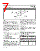
7 / 17 page  January 1995 7 Philips Semiconductors Product specification Frequency synthesizer HEF4750V LSI Fig.6 Phase characteristic of PC2. Strobe function The strobe function is intended for applications requiring extremely fast lock times. In normal operation the additional strobe input (STB) can be connected to the V-input and the circuit will function as described in the previous sections. In single, phase-locked-loop type frequency synthesizers, the comparison frequency generally used is either the nominal channel spacing or a sub-multiple. PC2 runs at the higher frequency (a higher reference frequency must also be used), whilst strobing takes place on the lower frequency, thereby obtaining a decrease in lock time. In a system using the Universal Divider HEF4751V, the output OFS cycles on the lower frequency, the output OFF cycles on the higher frequency. Out-of-lock function There are a number of situations in which the system goes from the locked to the out-of-lock state (OL goes HIGH): 1. When V’ leads R, however out of the range of PC1. 2. When R leads V’. 3. When an R-pulse is missing. 4. When a V-pulse is missing. 5. When two successive STB-commands occur, the first without corresponding V-signal. Phase modulator The phase modulator only uses one external capacitor, CB at pin TCB. A negative-going transition at the V-input causes CB to produce a positive-going linear ramp. When the ramp has reached a value almost equal to the modulation input voltage (at MOD), the ramp terminates, CB discharges and a start signal to the CA-ramp at TCA is produced. A linear phase modulation is reached in this way. If no modulation is required, the MOD-input must be connected to a fixed voltage of a certain positive value up to VDD. Care must be taken that the V’ pulse is never smaller than the minimum value to ensure that the external capacitor of PC1 (CA) can be discharged during that time. Since the V’ pulse width is directly related to the TCB ramp duration, there is a requirement for the minimum value of this ramp duration. Reference oscillator The reference oscillator normally operates with an external crystal as shown in Fig.2. The internal circuitry can be used as a buffer amplifier in case an external reference should be required. Reference divider The reference divider consists of a binary divider with a programmable division ratio of 1 to 1024 and a prescaler with selectable division ratios of 1, 2, 10 and 100, according to the following tables: Binary divider Prescaler N (A0 TO A9) DIVISION RATIO 0 1024 0 ≤ N ≤ 1023 N PROGRAMMING WORD (NS0, NS1) DIVISION RATIO 01 12 210 3 100 |
|
|
Link URL |
| Does ALLDATASHEET help your business so far? [ DONATE ] |
About Alldatasheet | Advertisement | Contact us | Privacy Policy | Link to Datasheet | Link Exchange | Manufacturer List All Rights Reserved©Alldatasheet.com |
| Russian : Alldatasheetru.com | Korean : Alldatasheet.co.kr | Spanish : Alldatasheet.es | French : Alldatasheet.fr | Italian : Alldatasheetit.com Portuguese : Alldatasheetpt.com | Polish : Alldatasheet.pl | Vietnamese : Alldatasheet.vn Indian : Alldatasheet.in | Mexican : Alldatasheet.com.mx | British : Alldatasheet.co.uk | New Zealand : Alldatasheet.co.nz |
|
Family Site : ic2ic.com |
icmetro.com |
 British ▼
 English
 Chinese
 German
 Japanese
 Russian
 Korean
 Spanish
 French
 Italian
 Portuguese
 Polish
 Vietnamese
 Indian
 Mexican
 British
 New Zealand