|
Electronic Components Datasheet Search |
|
|
Electronic Components Datasheet Search |
|
25AA512 Datasheet(PDF) 9 Page - Microchip Technology |
|
|
|||||||||||||||||||||||||||||
25AA512 Datasheet(HTML) 9 Page - Microchip Technology |
|
|
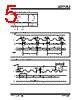
9 / 36 page  2010 Microchip Technology Inc. DS22021F-page 9 25AA512 2.2 Write Sequence Prior to any attempt to write data to the 25AA512, the write enable latch must be set by issuing the WREN instruction (Figure 2-4). This is done by setting CS low and then clocking out the proper instruction into the 25AA512. After all eight bits of the instruction are trans- mitted, the CS must be brought high to set the write enable latch. If the write operation is initiated immedi- ately after the WREN instruction without CS being brought high, the data will not be written to the array because the write enable latch will not have been properly set. A write sequence includes an automatic, self timed erase cycle. It is not required to erase any portion of the memory prior to issuing a WRITE instruction. Once the write enable latch is set, the user may proceed by setting the CS low, issuing a WRITE instruc- tion, followed by the 16-bit address, and then the data to be written. Up to 128 bytes of data can be sent to the device before a write cycle is necessary. The only restriction is that all of the bytes must reside in the same page. For the data to be actually written to the array, the CS must be brought high after the Least Significant bit (D0) of the nth data byte has been clocked in. If CS is brought high at any other time, the write operation will not be completed. Refer to Figure 2-2 and Figure 2-3 for more detailed illustrations on the byte write sequence and the page write sequence, respectively. While the write is in progress, the STATUS register may be read to check the status of the WPEN, WIP, WEL, BP1 and BP0 bits (Figure 2-6). A read attempt of a memory array location will not be possible during a write cycle. When the write cycle is completed, the write enable latch is reset. FIGURE 2-2: BYTE WRITE SEQUENCE Note: When doing a write of less than 128 bytes the data in the rest of the page is refreshed along with the data bytes being written. This will force the entire page to endure a write cycle, for this reason endurance is specified per page. Note: Page write operations are limited to writing bytes within a single physical page, regardless of the number of bytes actually being written. Physical page boundaries start at addresses that are integer multiples of the page buffer size (or ‘page size’), and end at addresses that are integer multiples of page size – 1. If a Page Write command attempts to write across a physical page boundary, the result is that the data wraps around to the beginning of the current page (overwriting data previously stored there), instead of being written to the next page as might be expected. It is therefore necessary for the application software to prevent page write operations that would attempt to cross a page boundary. SO SI CS 9 1011 2122 23242526 272829 30 31 00 0 0 0 0 01 15 14 13 12 21 0 7 654 321 0 Instruction 16-bit Address Data Byte High-Impedance SCK 0 2 34 567 1 8 Twc |
|
Link URL |
| Does ALLDATASHEET help your business so far? [ DONATE ] |
About Alldatasheet | Advertisement | Contact us | Privacy Policy | Link to Datasheet | Link Exchange | Manufacturer List All Rights Reserved©Alldatasheet.com |
| Russian : Alldatasheetru.com | Korean : Alldatasheet.co.kr | Spanish : Alldatasheet.es | French : Alldatasheet.fr | Italian : Alldatasheetit.com Portuguese : Alldatasheetpt.com | Polish : Alldatasheet.pl | Vietnamese : Alldatasheet.vn Indian : Alldatasheet.in | Mexican : Alldatasheet.com.mx | British : Alldatasheet.co.uk | New Zealand : Alldatasheet.co.nz |
|
Family Site : ic2ic.com |
icmetro.com |
 British ▼
 English
 Chinese
 German
 Japanese
 Russian
 Korean
 Spanish
 French
 Italian
 Portuguese
 Polish
 Vietnamese
 Indian
 Mexican
 British
 New Zealand