|
Electronic Components Datasheet Search |
|
|
Electronic Components Datasheet Search |
|
25AA512 Datasheet(PDF) 17 Page - Microchip Technology |
|
|
|||||||||||||||||||||||||||||
25AA512 Datasheet(HTML) 17 Page - Microchip Technology |
|
|
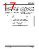
17 / 36 page  2010 Microchip Technology Inc. DS22021F-page 17 25AA512 2.10 CHIP ERASE The CHIP ERASE instruction will erase all bits (FFh) in the array. A Write Enable (WREN) instruction must be given prior to executing a CHIP ERASE. This is done by setting CS low and then clocking out the proper instruction into the 25AA512. After all eight bits of the instruction are transmitted, the CS must be brought high to set the write enable latch. The CHIP ERASE instruction is entered by driving the CS low, followed by the instruction code (Figure 2-10) onto the SI line. The CS pin must be driven high after the eighth bit of the instruction code has been given or the CHIP ERASE instruction will not be executed. Once the CS pin is driven high the self-timed CHIP ERASE instruc- tion begins. While the device is executing the CHIP ERASE instruction the WIP bit in the STATUS register can be read to determine when the CHIP ERASE instruction is complete. The CHIP ERASE instruction is ignored if either of the Block Protect bits (BP0, BP1) are not 0, meaning ¼, ½, or all of the array is protected. FIGURE 2-10: CHIP ERASE SEQUENCE SCK 0 2 34 56 7 1 SI High-Impedance SO CS 11 10 00 1 1 |
|
Link URL |
| Does ALLDATASHEET help your business so far? [ DONATE ] |
About Alldatasheet | Advertisement | Contact us | Privacy Policy | Link to Datasheet | Link Exchange | Manufacturer List All Rights Reserved©Alldatasheet.com |
| Russian : Alldatasheetru.com | Korean : Alldatasheet.co.kr | Spanish : Alldatasheet.es | French : Alldatasheet.fr | Italian : Alldatasheetit.com Portuguese : Alldatasheetpt.com | Polish : Alldatasheet.pl | Vietnamese : Alldatasheet.vn Indian : Alldatasheet.in | Mexican : Alldatasheet.com.mx | British : Alldatasheet.co.uk | New Zealand : Alldatasheet.co.nz |
|
Family Site : ic2ic.com |
icmetro.com |
 British ▼
 English
 Chinese
 German
 Japanese
 Russian
 Korean
 Spanish
 French
 Italian
 Portuguese
 Polish
 Vietnamese
 Indian
 Mexican
 British
 New Zealand