|
Electronic Components Datasheet Search |
|
|
Electronic Components Datasheet Search |
|
RF5765 Datasheet(PDF) 10 Page - RF Micro Devices |
|
|
|||||||||||||||||||||||||||||
RF5765 Datasheet(HTML) 10 Page - RF Micro Devices |
|
|
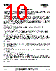
10 / 14 page  10 of 14 RF5765 DS120213 7628 Thorndike Road, Greensboro, NC 27409-9421 · For sales or technical support, contact RFMD at (+1) 336-678-5570 or sales-support@rfmd.com. Theory of Operation The RF5765 Front End Module (FEM) is designed for WiFi applications in the 2.5GHz ISM band. It can be applied in many por- table applications such as handsets, Portable Media Players, and portable battery power equipment. This highly integrated module can be connected directly to the battery without additional voltage regulators. WiFi TRANSMIT MODE The RF5765 requires a single positive supply (VCC), a positive supply for switch controls, and a regulated supply for the VREG to maintain nominal bias current. The RF5765 transmit path has a typical gain of 30dB from 2.4GHz to 2.5GHz, and delivers 20dBm typical output power under 54Mbps OFDM modulation and 23dBm under 1Mbps 11b modulation. The RF5765 con- tains basic filter components to produce a bandpass response for the transmit path. Due to space constraints inside the mod- ule, filtering is limited to a few resonant poles and additional filters may be required depending upon the end-user’s application. While in transmit mode, the active components are the Power Amplifier (PA) and the TX branch of the SP3T switch. Refer to the logic control table for proper settings. TX Biasing Instructions • Connect the TX input (pin-1) to a signal generator and a spectrum analyzer at the Antenna output (pin-10) •Set VCC to 3.3V with VREG set to 0V •Turn VREG ON and set voltage to 3.1V. VREG controls the current drawn by the PA and it should quickly reach a quiescent cur- rent of approximately 90mA±20mA. Care must be exercised not to exceed 3.5V on the VREG pin or the part may be dam- aged. • Control bias to the transmit branch of the SP3T switch is tied directly to VREG • The SP3T controls for the off branches (C_RX and C_BT) must be set to a logic “low” (0.2V max) or grounded. In the event that one of these branches is left floating or in a logic “high” the performance of the PA will degrade significantly. Likewise, unused RF Ports must be terminated in 50Ω to simulate actual system conditions and prevent RF signals from coupling back to the PA. •Turn RF ON WiFi RECEIVE MODE Within the frequency band of operation 2.4GHz to 2.5GHz, the RF5765 WiFi receive path has a typical gain of 18dB and a NF of 2.1dB with about 10mA of current. In RX mode, only the RX branch of the SP3T and the LNA are active. Refer to the logic control table for proper settings. RX Biasing Instructions • Connect the RX input (ANT/pin-10) to a signal generator and a spectrum analyzer at the RX output (pin-3). A VNA may be used as well. • Turn the LNA bias ON (pin-4) and set the voltage to 3.3V • Set C_RX (pin-6) high. This turns ON the receive branch of the SP3T. • The SP3T controls for the off branches (VREG and C_BT) must be set to a logic “low” (0.2V max) or grounded. In the event that one of these branches is left floating or in a logic “high” the performance will degrade. It is recommended to terminate unused RF Ports in 50Ω. • Set the control bias for the SPST switch (C_BWRX/pin-5) “low” during WiFi RX only mode. •Turn RF ON |
|
|
Link URL |
| Does ALLDATASHEET help your business so far? [ DONATE ] |
About Alldatasheet | Advertisement | Contact us | Privacy Policy | Link to Datasheet | Link Exchange | Manufacturer List All Rights Reserved©Alldatasheet.com |
| Russian : Alldatasheetru.com | Korean : Alldatasheet.co.kr | Spanish : Alldatasheet.es | French : Alldatasheet.fr | Italian : Alldatasheetit.com Portuguese : Alldatasheetpt.com | Polish : Alldatasheet.pl | Vietnamese : Alldatasheet.vn Indian : Alldatasheet.in | Mexican : Alldatasheet.com.mx | British : Alldatasheet.co.uk | New Zealand : Alldatasheet.co.nz |
|
Family Site : ic2ic.com |
icmetro.com |
 British ▼
 English
 Chinese
 German
 Japanese
 Russian
 Korean
 Spanish
 French
 Italian
 Portuguese
 Polish
 Vietnamese
 Indian
 Mexican
 British
 New Zealand