|
Electronic Components Datasheet Search |
|
|
Electronic Components Datasheet Search |
|
ADP5072ACBZ-R7 Datasheet(PDF) 15 Page - Analog Devices |
|
|
|||||||||||||||||||||||||||||
ADP5072ACBZ-R7 Datasheet(HTML) 15 Page - Analog Devices |
|
|
15 / 24 page 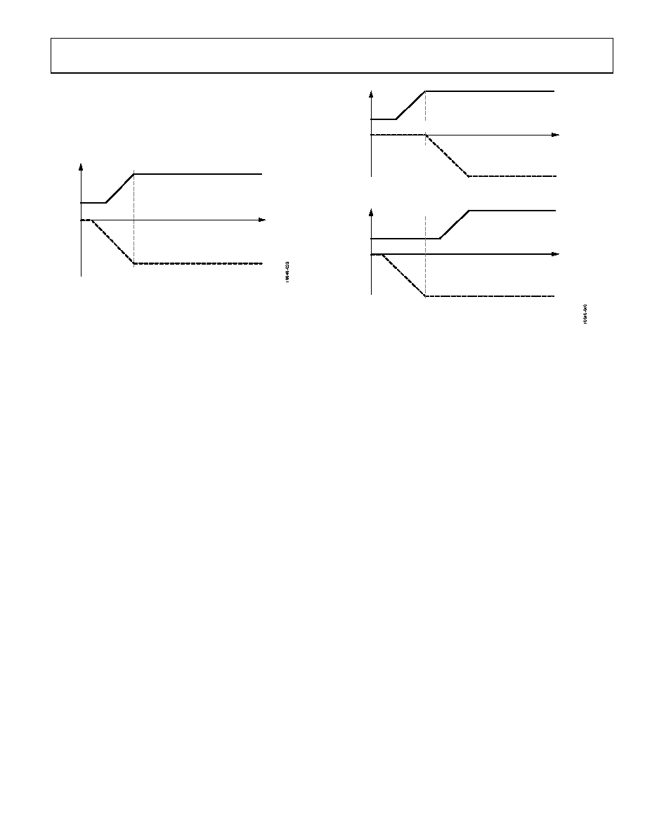 Data Sheet ADP5072 Rev. 0 | Page 15 of 24 To configure the simultaneous enable mode, connect the SEQ pin to the PVIN pin. Both regulators power up simultaneously when the EN2 pin is taken high. The EN1 pin enable can be used to enable the internal references ahead of enabling the outputs, if desired. The simultaneous enable mode timing is shown in Figure 41. VIN VPOS TIME VNEG SIMULTANEOUS ENABLE MODE (SEQ = HIGH, EN2 = HIGH) Figure 41. Simultaneous Enable Mode To configure the sequential enable mode, pull the SEQ pin low. In this mode, either VPOS or VNEG can be enabled first by using the EN1 pin or EN2 pin. Keep the other pin low. The secondary supply is enabled when the primary supply completes soft start and its feedback voltage reaches approximately 85% of the target value. The sequential enable mode timing is shown in Figure 42. TIME TIME VPOS VNEG VPOS VNEG 1. VPOS FOLLOWED BY VNEG (SEQ = LOW, EN1 = HIGH, EN2 = LOW) 2. VNEG FOLLOWED BY VPOS (SEQ = LOW, EN2 = HIGH, EN1 = LOW) VIN VIN Figure 42. Sequential Enable Mode |
|
|
Link URL |
| Does ALLDATASHEET help your business so far? [ DONATE ] |
About Alldatasheet | Advertisement | Contact us | Privacy Policy | Link to Datasheet | Link Exchange | Manufacturer List All Rights Reserved©Alldatasheet.com |
| Russian : Alldatasheetru.com | Korean : Alldatasheet.co.kr | Spanish : Alldatasheet.es | French : Alldatasheet.fr | Italian : Alldatasheetit.com Portuguese : Alldatasheetpt.com | Polish : Alldatasheet.pl | Vietnamese : Alldatasheet.vn Indian : Alldatasheet.in | Mexican : Alldatasheet.com.mx | British : Alldatasheet.co.uk | New Zealand : Alldatasheet.co.nz |
|
Family Site : ic2ic.com |
icmetro.com |
 British ▼
 English
 Chinese
 German
 Japanese
 Russian
 Korean
 Spanish
 French
 Italian
 Portuguese
 Polish
 Vietnamese
 Indian
 Mexican
 British
 New Zealand