4 / 54 page

NT7502
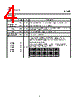
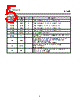
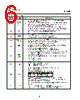
Pad Description
Power Supply
Pad No.
Symbol
I/O
Descriptions
30 - 33
VDD
Supply
2.4 - 3.5V power supply input. These pads must be connected each other
10, 16, 26, 53, 71,
77, 81, 91
VDD
Supply
2.4 - 3.5V power supply output for pad option
34 - 36
VDD2
Supply
This is the reference power supply for the step-up voltage circuit for the LCD.
These pads must be connected each other
37 - 40
VSS
Supply
Ground. These pads must be connected each other
7, 13, 25, 29 , 56,
69 - 70, 74, 79, 83
VSS
Supply
Ground output for pad option
65 - 66
57 - 58
59 - 60
61 - 62
63 - 64
V0
V1
V2
V3
V4
Supply
LCD driver supply voltages. The voltage determined by LCD cell is
impedance-converted by a resistive driver or an operation amplifier for
application. Voltages should be according to the following relationship:
V0
≥ V1 ≥ V2 ≥ V3 ≥ V4 ≥ VSS
When the on-chip operating power circuit is on, the following voltages
are supplied to V1 to V4 by the on-chip power circuit. Voltage selection is
performed by the Set LCD Bias command.
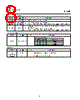
LCD bias
V1
V2
V3
V4
1/5 bias
4/5V0
3/5V0
2/5V0
1/5V0
1/6 bias
5/6V0
4/6V0
2/6V0
1/6V0
1/7 bias
6/7V0
5/7V0
2/7V0
1/7V0
1/8 bias
7/8V0
6/8V0
2/8V0
1/8V0
1/9 bias
8/9V0
7/9V0
2/9V0
1/9V0
4

 British ▼
 English
 Chinese
 German
 Japanese
 Russian
 Korean
 Spanish
 French
 Italian
 Portuguese
 Polish
 Vietnamese
 Indian
 Mexican
 British
 New Zealand