|
Electronic Components Datasheet Search |
|
|
Electronic Components Datasheet Search |
|
MPC93R52 Datasheet(PDF) 3 Page - Motorola, Inc |
|
|
|||||||||||||||||||||||||||||
MPC93R52 Datasheet(HTML) 3 Page - Motorola, Inc |
|
|
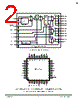
3 / 16 page  MPC93R52 TIMING SOLUTIONS 3 MOTOROLA Table 1: PIN CONFIGURATION Pin I/O Type Function CCLK Input LVCMOS PLL reference clock signal FB_IN Input LVCMOS PLL feedback signal input, connect to an output F_RANGE Input LVCMOS PLL frequency range select FSELA Input LVCMOS Frequency divider select for bank A outputs FSELB Input LVCMOS Frequency divider select for bank B outputs FSELC Input LVCMOS Frequency divider select for bank C outputs PLL_EN Input LVCMOS PLL enable/disable MR/OE Input LVCMOS Output enable/disable (high–impedance tristate) and device reset QA0–4, QB0–3, QC0–1 Output LVCMOS Clock outputs GND Supply Ground Negative power supply VCCA Supply VCC PLL positive power supply (analog power supply). It is recommended to use an external RC filter for the analog power supply pin VCCA. Please see applications section for details. VCC Supply VCC Positive power supply for I/O and core Table 2: FUNCTION TABLE Control Default 0 1 F_RANGE, FSELA, FSELB, and FSELC control the operating PLL frequency range and input/output frequency ratios. See Table 1 and Table 2 for supported frequency ranges and output to input frequency ratios. F_RANGE 0 VCO ÷ 1 (High input frequency range) VCO ÷ 2 (Low input frequency range) FSELA 0 Output divider ÷ 4 Output divider ÷ 6 FSELB 0 Output divider ÷ 4 Output divider ÷ 2 FSELC 0 Output divider ÷ 2 Output divider ÷ 4 MR/OE 0 Outputs enabled (active) Outputs disabled (high–impedance state) and reset of the device. During reset, the PLL feedback loop is open and the VCO is operating at its lowest frequency. The MPC93R52 requires reset after any loss of PLL lock. Loss of PLL lock may occur when the external feedback path is interrupted. The length of the reset pulse should be greater than two reference clock cycles (CCLK). The device is reset by the internal power–on reset (POR) circuitry during power–up. PLL_EN 0 Normal operation mode with PLL enabled. Test mode with PLL disabled. CCLK is substituted for the internal VCO output. MPC93R52 is fully static and no minimum frequency limit applies. All PLL related AC characteristics are not applicable. |
|
|
Link URL |
| Does ALLDATASHEET help your business so far? [ DONATE ] |
About Alldatasheet | Advertisement | Contact us | Privacy Policy | Link to Datasheet | Link Exchange | Manufacturer List All Rights Reserved©Alldatasheet.com |
| Russian : Alldatasheetru.com | Korean : Alldatasheet.co.kr | Spanish : Alldatasheet.es | French : Alldatasheet.fr | Italian : Alldatasheetit.com Portuguese : Alldatasheetpt.com | Polish : Alldatasheet.pl | Vietnamese : Alldatasheet.vn Indian : Alldatasheet.in | Mexican : Alldatasheet.com.mx | British : Alldatasheet.co.uk | New Zealand : Alldatasheet.co.nz |
|
Family Site : ic2ic.com |
icmetro.com |
 British ▼
 English
 Chinese
 German
 Japanese
 Russian
 Korean
 Spanish
 French
 Italian
 Portuguese
 Polish
 Vietnamese
 Indian
 Mexican
 British
 New Zealand