|
Electronic Components Datasheet Search |
|
|
Electronic Components Datasheet Search |
|
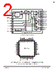
MPC93R52 Datasheet(PDF) 5 Page - Motorola, Inc |
|
|
|||||||||||||||||||||||||||||
MPC93R52 Datasheet(HTML) 5 Page - Motorola, Inc |
|
|
5 / 16 page  MPC93R52 TIMING SOLUTIONS 5 MOTOROLA Table 6: AC CHARACTERISTICS (VCC = 3.3V ± 5%, TA = 0° to 70°C)a Symbol Characteristics Min Typ Max Unit Condition fref Input reference frequency in PLL modebc ÷4 feedback ÷6 feedback ÷8 feedback ÷12 feedback Input reference frequency in PLL bypass moded 50.0 33.3 25.0 16.67 50.0 120.0 80.0 60.0 40.0 250.0 MHz MHz MHz MHz MHz fVCO VCO lock frequency rangee 200 480 MHz fMAX Output Frequency ÷2 outputf ÷4 output ÷6 output ÷8 output ÷12 output 100 50 33.3 25 16.67 240 120 80 60 40 MHz MHz MHz MHz MHz tPWMIN Minimum Reference Input Pulse Width 2.0 ns tr, tf CCLK Input Rise/Fall Timeg 1.0 ns 0.8 to 2.0V t( ∅) Propagation Delay CCLK to FB_IN (fref = 50MHz) (static phase offset) -100 +200 ps ps PLL locked tsk(O) Output-to-output Skewh all outputs, any frequency within QA output bank within QB output bank within QC output bank 150 100 100 50 ps ps ps ps DC Output duty cycle 47 50 53 % tr, tf Output Rise/Fall Time 0.1 1.0 ns 0.55 to 2.4V tPLZ, HZ Output Disable Time 8 ns tPZL, LZ Output Enable Time 10 ns tJIT(CC) Cycle-to-cycle jitter output frequencies mixed all outputs same frequency 450 100 ps ps tJIT(PER) Period Jitter output frequencies mixed all outputs same frequency 450 100 ps ps tJIT( ∅) I/O Phase Jitteri ÷4 feedback divider RMS (1 σ) ÷6 feedback divider RMS (1 σ) ÷8 feedback divider RMS (1 σ) ÷12 feedback divider RMS (1 σ) 40 50 60 80 ps ps ps ps BW PLL closed loop bandwidthj ÷4 feedback ÷6 feedback ÷8 feedback ÷12 feedback 2.0–8.0 1.0–4.0 0.8–2.5 0.6–1.5 MHz MHz MHz MHz tLOCK Maximum PLL Lock Time 10 ms a AC characteristics apply for parallel output termination of 50 Ω to VTT. b PLL mode requires PLL_EN=0 to enable the PLL and zero-delay operation. c The PLL may be unstable with a divide by 2 feedback ratio. d In PLL bypass mode, the MPC93R52 divides the input reference clock. e The input frequency fref on CCLK must match the VCO frequency range divided by the feedback divider ratio FB: fref = fVCO ÷ FB. f See Table 9 and Table 10 for output divider configurations. g The MPC93R52 will operate with input rise and fall times up to 3.0 ns, but the AC characteristics, specifically t( ∅), can only be guaranteed if tr/tf are within the specified range. h See application section for part-to-part skew calculation. i See application section for a jitter calculation for other confidence factors than 1 s. j -3 dB point of PLL transfer characteristics. |
|
|
Link URL |
| Does ALLDATASHEET help your business so far? [ DONATE ] |
About Alldatasheet | Advertisement | Contact us | Privacy Policy | Link to Datasheet | Link Exchange | Manufacturer List All Rights Reserved©Alldatasheet.com |
| Russian : Alldatasheetru.com | Korean : Alldatasheet.co.kr | Spanish : Alldatasheet.es | French : Alldatasheet.fr | Italian : Alldatasheetit.com Portuguese : Alldatasheetpt.com | Polish : Alldatasheet.pl | Vietnamese : Alldatasheet.vn Indian : Alldatasheet.in | Mexican : Alldatasheet.com.mx | British : Alldatasheet.co.uk | New Zealand : Alldatasheet.co.nz |
|
Family Site : ic2ic.com |
icmetro.com |
 British ▼
 English
 Chinese
 German
 Japanese
 Russian
 Korean
 Spanish
 French
 Italian
 Portuguese
 Polish
 Vietnamese
 Indian
 Mexican
 British
 New Zealand