 |
Electronic Components Datasheet Search |
|
|
Electronic Components Datasheet Search |
|
The question interval is too short.
Please try again in a few seconds.

Hello, Please ask a question about MPM3686 Datasheet
# Example questions:
➢ Describe the path of the feedback signal from the output to the pwm modulator. what components are involved in this process?
➢ What is the typical soft-start time, as indicated in the block diagram, and what components influence this timing?
➢ What components in the block diagram contribute to over-voltage (ov) and under-voltage (uv) protection, and how do they function?
| Part No. | MPM3686 |
| Manufacturer | MPS |
| Size | 2Mb |
| Pages | 19 pages |
| Description | 18V 20A Step-Down Power Module in 12x15x4mm QFN |




1. Overview & Functionality
️· What it is: The MPM3686 is a synchronous buck-boost DC-DC converter. This means it can regulate the output voltage *above* or *below* the input voltage. This is a significant advantage in applications where the input voltage can vary considerably.
️· Synchronous: This means it uses MOSFETs (rather than diodes) for both the high-side and low-side switching elements. This significantly improves efficiency compared to asynchronous converters.
️· Key Applications: Suitable for a wide range of applications including battery-powered devices, LED drivers, and systems requiring regulated voltage from variable sources.
2. Electrical Specifications & Key Features
️· Input Voltage Range: Not explicitly stated in the extract, but implied to be quite flexible due to the buck-boost nature.
️· Output Voltage: Adjustable (through external components, see trimming section)
️· Switching Frequency: Not specifically mentioned, but typically in the range of 100kHz - 1MHz for power converters of this type.
️· Efficiency: High efficiency, especially important for battery-powered applications.
️· Features:
- Buck-Boost Topology: Handles input voltages above and below the desired output voltage.
- Synchronous Rectification: Uses MOSFETs for lower losses.
- Soft Start: Controls inrush current during startup, preventing damage and improving stability.
- Overvoltage Protection (OVP): Shuts down the converter if the output voltage exceeds a safe level.
- UVLO (Undervoltage Lockout): Prevents operation if the input voltage is too low.
- Current Limit: Protects the converter from overcurrent conditions.
- Adjustable Output Voltage: Allows customization for specific application needs.
- Trimability: Allows fine-tuning of the output voltage using external resistors.
- Power Good (PGOOD) Output: Indicates when the output voltage is within a specified range.
3. Block Diagram Breakdown (Most Important for Design)
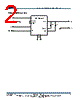
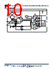
The block diagram is crucial to understand how the converter works. Here's an explanation of the key blocks:
️· HS/LS Driver & FETs: High-side and Low-side drivers control the MOSFETs (HS-FET, LS-FET). These MOSFETs perform the actual power conversion.
️· ZCD Current/Modulator: Zero-Current Detection (ZCD) is essential for buck-boost operation. It optimizes efficiency by ensuring the MOSFETs switch near zero current. The modulator generates the PWM (Pulse Width Modulation) signal to control the switching frequency.
️· LOGIC: Implements the control algorithms including soft-start, current limiting, UVLO, OVP, and PGOOD.
️· Reference & VCC/LDO: Provides a stable reference voltage for the control circuit and regulates the internal voltage.
️· ON/OFF Timer: Manages the soft-start process and determines the duty cycle.
️· FB Comparator: Compares the output voltage (via a feedback network) to the reference voltage and generates the error signal that drives the modulator.
️· BST Bias: Generates the gate voltage for the high-side MOSFET.
4. Important Design Considerations (Based on the Extract)
️· Feedback Network: The output voltage is determined by a resistor divider network. Carefully choose resistor values for desired output voltage.
️· Soft Start Components: The soft-start capacitors and resistors need to be selected to achieve the desired inrush current limiting.
️· Feedback Compensation: The control loop must be properly compensated to ensure stability. This usually involves adding capacitors and resistors to the feedback path.
️· External Components: The data sheet will have specific recommendations for external components, including MOSFETs, inductors, and capacitors.
️· Trimming: Resistors can be used to fine-tune the output voltage to achieve the exact value required.
️· Layout: Proper PCB layout is crucial for high-frequency power converters to minimize noise, parasitic inductance, and signal integrity issues.
5. What's Missing from the Extract
️· Detailed Pin Descriptions: A comprehensive list of pin functions and their characteristics.
️· Typical Application Circuits: Example circuits showing how to connect external components.
️· Component Selection Guide: Recommendations for specific MOSFETs, inductors, and capacitors.
️· Detailed Timing Diagrams: Visual representations of the converter's operation.
️· Thermal Management Information: Guidelines for heat sinking and thermal design.
1. Overview & Functionality
️· What it is: The MPM3686 is a synchronous buck-boost DC-DC converter. This means it can regulate the output voltage *above* or *below* the input voltage. This is a significant advantage in applications where the input voltage can vary considerably.
️· Synchronous: This means it uses MOSFETs (rather than diodes) for both the high-side and low-side switching elements. This significantly improves efficiency compared to asynchronous converters.
️· Key Applications: Suitable for a wide range of applications including battery-powered devices, LED drivers, and systems requiring regulated voltage from variable sources.
2. Electrical Specifications & Key Features
️· Input Voltage Range: Not explicitly stated in the extract, but implied to be quite flexible due to the buck-boost nature.
️· Output Voltage: Adjustable (through external components, see trimming section)
️· Switching Frequency: Not specifically mentioned, but typically in the range of 100kHz - 1MHz for power converters of this type.
️· Efficiency: High efficiency, especially important for battery-powered applications.
️· Features:
- Buck-Boost Topology: Handles input voltages above and below the desired output voltage.
- Synchronous Rectification: Uses MOSFETs for lower losses.
- Soft Start: Controls inrush current during startup, preventing damage and improving stability.
- Overvoltage Protection (OVP): Shuts down the converter if the output voltage exceeds a safe level.
- UVLO (Undervoltage Lockout): Prevents operation if the input voltage is too low.
- Current Limit: Protects the converter from overcurrent conditions.
- Adjustable Output Voltage: Allows customization for specific application needs.
- Trimability: Allows fine-tuning of the output voltage using external resistors.
- Power Good (PGOOD) Output: Indicates when the output voltage is within a specified range.
3. Block Diagram Breakdown (Most Important for Design)
The block diagram is crucial to understand how the converter works. Here's an explanation of the key blocks:
️· HS/LS Driver & FETs: High-side and Low-side drivers control the MOSFETs (HS-FET, LS-FET). These MOSFETs perform the actual power conversion.
️· ZCD Current/Modulator: Zero-Current Detection (ZCD) is essential for buck-boost operation. It optimizes efficiency by ensuring the MOSFETs switch near zero current. The modulator generates the PWM (Pulse Width Modulation) signal to control the switching frequency.
️· LOGIC: Implements the control algorithms including soft-start, current limiting, UVLO, OVP, and PGOOD.
️· Reference & VCC/LDO: Provides a stable reference voltage for the control circuit and regulates the internal voltage.
️· ON/OFF Timer: Manages the soft-start process and determines the duty cycle.
️· FB Comparator: Compares the output voltage (via a feedback network) to the reference voltage and generates the error signal that drives the modulator.
️· BST Bias: Generates the gate voltage for the high-side MOSFET.
4. Important Design Considerations (Based on the Extract)
️· Feedback Network: The output voltage is determined by a resistor divider network. Carefully choose resistor values for desired output voltage.
️· Soft Start Components: The soft-start capacitors and resistors need to be selected to achieve the desired inrush current limiting.
️· Feedback Compensation: The control loop must be properly compensated to ensure stability. This usually involves adding capacitors and resistors to the feedback path.
️· External Components: The data sheet will have specific recommendations for external components, including MOSFETs, inductors, and capacitors.
️· Trimming: Resistors can be used to fine-tune the output voltage to achieve the exact value required.
️· Layout: Proper PCB layout is crucial for high-frequency power converters to minimize noise, parasitic inductance, and signal integrity issues.
5. What's Missing from the Extract
️· Detailed Pin Descriptions: A comprehensive list of pin functions and their characteristics.
️· Typical Application Circuits: Example circuits showing how to connect external components.
️· Component Selection Guide: Recommendations for specific MOSFETs, inductors, and capacitors.
️· Detailed Timing Diagrams: Visual representations of the converter's operation.
️· Thermal Management Information: Guidelines for heat sinking and thermal design.
| Part No. | MPM3686 |
| Manufacturer | MPS |
| Size | 2Mb |
| Pages | 19 pages |
| Description | 18V 20A Step-Down Power Module in 12x15x4mm QFN |
| Does ALLDATASHEET help your business so far? [ DONATE ] |
About Alldatasheet | Advertisement | Contact us | Privacy Policy | Link to Datasheet | Link Exchange | Manufacturer List All Rights Reserved©Alldatasheet.com |
| Russian : Alldatasheetru.com | Korean : Alldatasheet.co.kr | Spanish : Alldatasheet.es | French : Alldatasheet.fr | Italian : Alldatasheetit.com Portuguese : Alldatasheetpt.com | Polish : Alldatasheet.pl | Vietnamese : Alldatasheet.vn Indian : Alldatasheet.in | Mexican : Alldatasheet.com.mx | British : Alldatasheet.co.uk | New Zealand : Alldatasheet.co.nz |
|
Family Site : ic2ic.com |
icmetro.com |
 British ▼
  English
 Chinese
 German
 Japanese
 Russian
 Korean
 Spanish
 French
 Italian
 Portuguese
 Polish
 Vietnamese
 Indian
 Mexican
 New Zealand