|
Electronic Components Datasheet Search |
|
|
Electronic Components Datasheet Search |
|
MPM3686 Datasheet(PDF) 17 Page - Monolithic Power Systems |
|
|
|||||||||||||||||||||||||||||
MPM3686 Datasheet(HTML) 17 Page - Monolithic Power Systems |
|
|
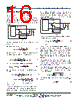
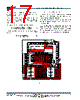
17 / 19 page  MPM3686 – 18V 20A STEP-DOWN POWER MODULE MPM3686 Rev. 1.02 www.MonolithicPower.com 17 10/13/2016 MPS Proprietary Information. Patent Protected. Unauthorized Photocopy and Duplication Prohibited. © 2016 MPS. All Rights Reserved. For simplification, choose an input capacitor with an RMS current rating that exceeds half the maximum load current. The input capacitance value determines the converter input voltage ripple. Select a capacitor value that meets any input voltage ripple requirements. Estimate the input voltage ripple as follows: ) V V 1 ( V V C F I V IN OUT IN OUT IN SW OUT IN (18) The worst-case condition occurs at VIN = 2VOUT, where: IN SW OUT IN C F I 4 1 V (19) PCB Layout Recommendations 1. Place the input/output capacitors on the same side of the MPM3686, and as close to the MPM3686 package as possible. 2. A solid system ground layer is required to be placed immediately below the surface layer with the MPM3686. 3. Thermal VIAs (18 mil diameter and 8 mil hole size) are required to be placed underneath the GND, IN and VOUT pads, as well as the edges of the MPM3686 and the input/output capacitors. 4. Keep the DC_trim traces as short as possible. Figure 10 CIN1 CIN2 COUT1 COUT2 SW Rtrim Ctrim IN VOUT GND COUT3 CIN3 PG VCC AGND SS AGND EN >FERQ VIN DC_trim> FREQ> AGND N/C BST VOUT SW SW SW SW N/C VOUT VOUT VOUT VOUT VOUT VOUT SW |
|
|
Link URL |
| Does ALLDATASHEET help your business so far? [ DONATE ] |
About Alldatasheet | Advertisement | Contact us | Privacy Policy | Link to Datasheet | Link Exchange | Manufacturer List All Rights Reserved©Alldatasheet.com |
| Russian : Alldatasheetru.com | Korean : Alldatasheet.co.kr | Spanish : Alldatasheet.es | French : Alldatasheet.fr | Italian : Alldatasheetit.com Portuguese : Alldatasheetpt.com | Polish : Alldatasheet.pl | Vietnamese : Alldatasheet.vn Indian : Alldatasheet.in | Mexican : Alldatasheet.com.mx | British : Alldatasheet.co.uk | New Zealand : Alldatasheet.co.nz |
|
Family Site : ic2ic.com |
icmetro.com |
 British ▼
 English
 Chinese
 German
 Japanese
 Russian
 Korean
 Spanish
 French
 Italian
 Portuguese
 Polish
 Vietnamese
 Indian
 Mexican
 British
 New Zealand