|
Electronic Components Datasheet Search |
|
|
Electronic Components Datasheet Search |
|
NL17SG373 Datasheet(PDF) 2 Page - ON Semiconductor |
|
|
|||||||||||||||||||||||||||||
NL17SG373 Datasheet(HTML) 2 Page - ON Semiconductor |
|
|
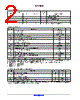
2 / 10 page  NL17SG373 www.onsemi.com 2 FUNCTION TABLE Input Internal Latch Output Operating Mode OE LE D Q L H L L L Enable and Read Register L H H H H (Transparent Mode) L L X L L Latch and Read Register L L X H H H X X X Z Latch Register and Disable Output MAXIMUM RATINGS Symbol Parameter Value Unit VCC DC Supply Voltage −0.5 to +5.5 V VIN DC Input Voltage −0.5 to +5.5 V VOUT DC Output Voltage −0.5 to VCC + 0.5 V IIK DC Input Diode Current VIN < GND −50 mA IOK DC Output Diode Current VOUT < GND, VOUT > VCC ±50 mA IO DC Output Source/Sink Current ±20 mA ICC DC Supply Current Per Supply Pin ±50 mA IGND DC Ground Current per Ground Pin ±50 mA TSTG Storage Temperature Range −65 to +150 °C TL Lead Temperature, 1 mm from Case for 10 Seconds 260 °C TJ Junction Temperature Under Bias 150 °C MSL Moisture Sensitivity Level 1 FR Flammability Rating Oxygen Index: 28 to 34 UL 94 V−0 @ 0.125 in VESD ESD Withstand Voltage Human Body Mode (Note 2) Machine Model (Note 3) > 3000 > 200 V ILATCHUP Latchup Performance Above VCC and Below GND at 125°C (Note 4) ±100 mA Stresses exceeding those listed in the Maximum Ratings table may damage the device. If any of these limits are exceeded, device functionality should not be assumed, damage may occur and reliability may be affected. 1. Measured with minimum pad spacing on an FR4 board, using 10 mm−by−1 inch, 2 ounce copper trace no air flow. 2. Tested to EIA / JESD22−A114−A. 3. Tested to EIA / JESD22−A115−A. 4. Tested to EIA / JESD78. RECOMMENDED OPERATING CONDITIONS Symbol Parameter Min Max Unit VCC Positive DC Supply Voltage 0.9 3.6 V VIN Digital Input Voltage 0 3.6 V VOUT Output Voltage Active Mode 0 VCC V TA Operating Free−Air Temperature −55 +125 °C Dt / DV Input Transition Rise or Fail Rate VCC = 3.3 V ± 0.3 V 0 10 nS/V Functional operation above the stresses listed in the Recommended Operating Ranges is not implied. Extended exposure to stresses beyond the Recommended Operating Ranges limits may affect device reliability. |
|
|
Link URL |
| Does ALLDATASHEET help your business so far? [ DONATE ] |
About Alldatasheet | Advertisement | Contact us | Privacy Policy | Link to Datasheet | Link Exchange | Manufacturer List All Rights Reserved©Alldatasheet.com |
| Russian : Alldatasheetru.com | Korean : Alldatasheet.co.kr | Spanish : Alldatasheet.es | French : Alldatasheet.fr | Italian : Alldatasheetit.com Portuguese : Alldatasheetpt.com | Polish : Alldatasheet.pl | Vietnamese : Alldatasheet.vn Indian : Alldatasheet.in | Mexican : Alldatasheet.com.mx | British : Alldatasheet.co.uk | New Zealand : Alldatasheet.co.nz |
|
Family Site : ic2ic.com |
icmetro.com |
 British ▼
 English
 Chinese
 German
 Japanese
 Russian
 Korean
 Spanish
 French
 Italian
 Portuguese
 Polish
 Vietnamese
 Indian
 Mexican
 British
 New Zealand