|
Electronic Components Datasheet Search |
|
|
Electronic Components Datasheet Search |
|
ADAR4002ACPZ-R7 Datasheet(PDF) 48 Page - Analog Devices |
|
|
|||||||||||||||||||||||||||||
ADAR4002ACPZ-R7 Datasheet(HTML) 48 Page - Analog Devices |
|
|
48 / 66 page 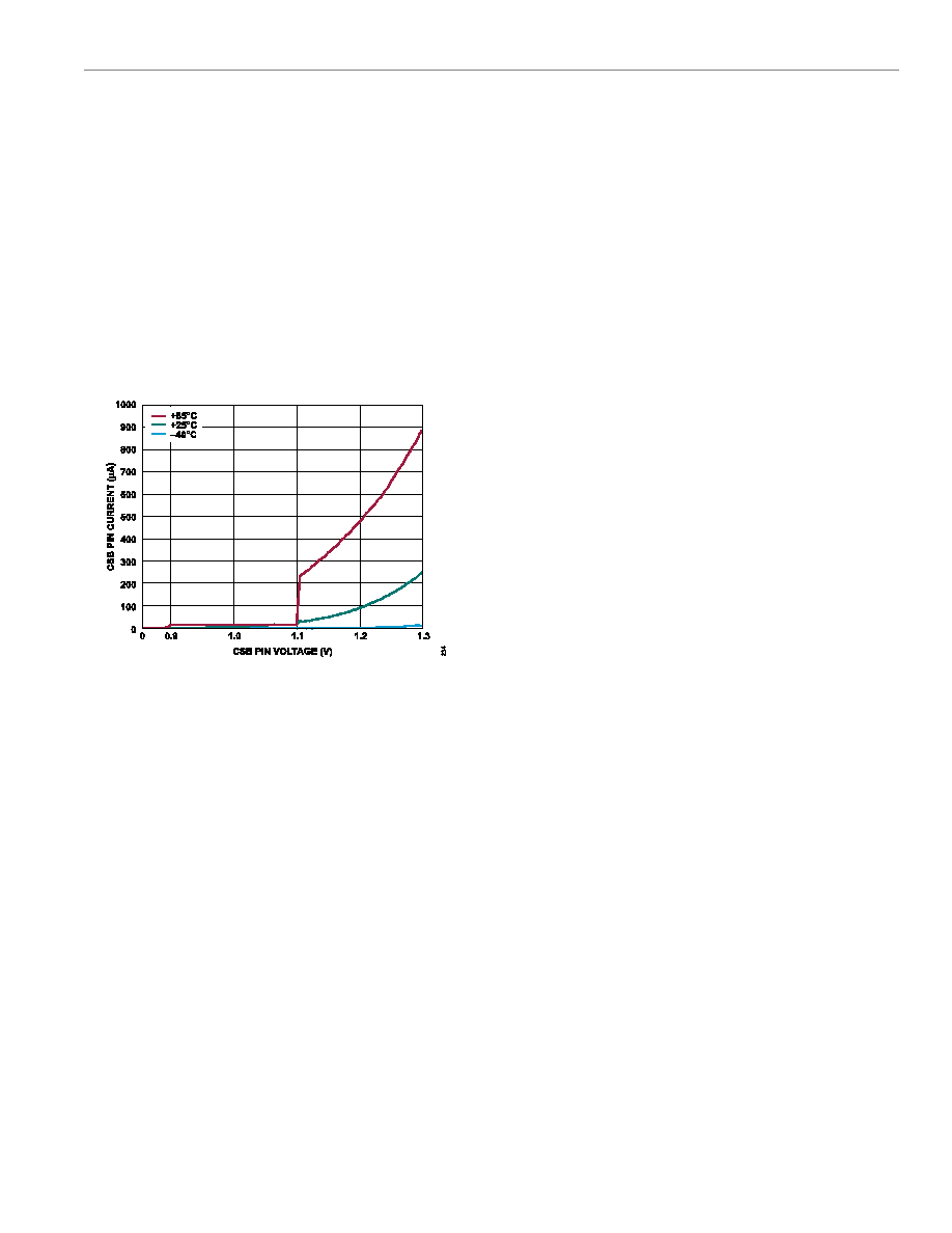 Data Sheet ADAR4002 APPLICATIONS INFORMATION analog.com Rev. A | 48 of 66 LOGIC VOLTAGES GREATER THAN 1.2 V Driving CSB/CLKO and DATA_IO to voltages more than 1.2 V, appreciable current sinks into the pin, especially over temperature (see Figure 133). Keep voltage drive levels to 1.2 V or lower on these bidirectional, dual-use pins to avoid high-current draw. The high-current draw is especially pronounced for the CSB/CLKO pin in SPI mode. The CSB/CLKO pin idles high between SPI writes; therefore, high-current draw occurs between SPI writes if the drive voltage is more than 1.2 V. The digital input only pins, CLK_IN, MODE, and UPDATE, do not draw high current when driven with larger voltages than 1.2 V. However, 1.2 V is still the recommend operational maximum for these input pins. Figure 133. CSB Pin Current vs. CSB Pin Voltage Drive Level over Tempera- ture While in SPI Mode |
|
Link URL |
| Does ALLDATASHEET help your business so far? [ DONATE ] |
About Alldatasheet | Advertisement | Contact us | Privacy Policy | Link to Datasheet | Link Exchange | Manufacturer List All Rights Reserved©Alldatasheet.com |
| Russian : Alldatasheetru.com | Korean : Alldatasheet.co.kr | Spanish : Alldatasheet.es | French : Alldatasheet.fr | Italian : Alldatasheetit.com Portuguese : Alldatasheetpt.com | Polish : Alldatasheet.pl | Vietnamese : Alldatasheet.vn Indian : Alldatasheet.in | Mexican : Alldatasheet.com.mx | British : Alldatasheet.co.uk | New Zealand : Alldatasheet.co.nz |
|
Family Site : ic2ic.com |
icmetro.com |
 British ▼
 English
 Chinese
 German
 Japanese
 Russian
 Korean
 Spanish
 French
 Italian
 Portuguese
 Polish
 Vietnamese
 Indian
 Mexican
 British
 New Zealand