|
Electronic Components Datasheet Search |
|
|
Electronic Components Datasheet Search |
|
MB9BF412R Datasheet(PDF) 57 Page - SPANSION |
|
|
|||||||||||||||||||||||||||||
MB9BF412R Datasheet(HTML) 57 Page - SPANSION |
|
|
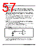
57 / 121 page 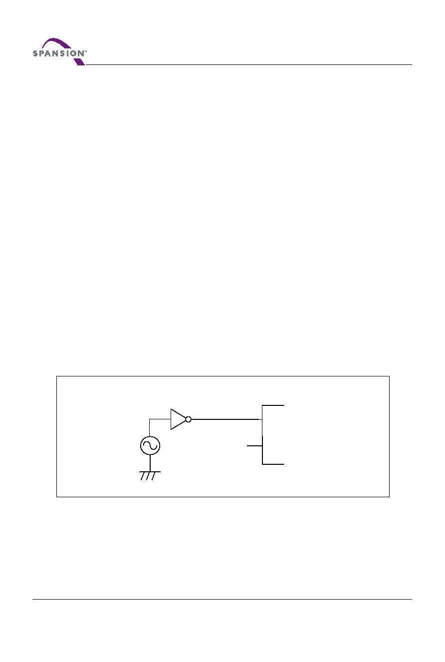 D a t a S h e e t 54 MB9B410R-DS706-00026-3v0-E, March 11, 2015 CONFIDENTIAL Handling Devices Power supply pins In products with multiple VCC and VSS pins, respective pins at the same potential are interconnected within the device in order to prevent malfunctions such as latch-up. However, all of these pins should be connected externally to the power supply or ground lines in order to reduce electromagnetic emission levels, to prevent abnormal operation of strobe signals caused by the rise in the ground level, and to conform to the total output current rating. Moreover, connect the current supply source with each POWER pins and GND pins of this device at low impedance. It is also advisable that a ceramic capacitor of approximately 0.1 µF be connected as a bypass capacitor between each Power supply pin and GND pin, between AVCC pin and AVSS pin near this device. Stabilizing power supply voltage A malfunction may occur when the power supply voltage fluctuates rapidly even though the fluctuation is within the recommended operating conditions of the VCC power supply voltage. As a rule, with voltage stabilization, suppress the voltage fluctuation so that the fluctuation in VCC ripple (peak-to-peak value) at the commercial frequency (50 Hz/60 Hz) does not exceed 10% of the VCC value in the recommended operating conditions, and the transient fluctuation rate does not exceed 0.1 V/μs when there is a momentary fluctuation on switching the power supply. Crystal oscillator circuit Noise near the X0/X1 and X0A/X1A pins may cause the device to malfunction. Design the printed circuit board so that X0/X1, X0A/X1A pins, the crystal oscillator (or ceramic oscillator), and the bypass capacitor to ground are located as close to the device as possible. It is strongly recommended that the PC board artwork be designed such that the X0/X1 and X0A/X1A pins are surrounded by ground plane as this is expected to produce stable operation. Evaluate oscillation of your using crystal oscillator by your mount board. Using an external clock When using an external clock, the clock signal should be input to the X0, X0A pin only and the X1, X1A pin should be kept open. Handling when using Multi-function serial pin as I 2C pin If it is using multi-function serial pin as I 2C pins, P-ch transistor of digital output is always disable. However, I 2C pins need to keep the electrical characteristic like other pins and not to connect to external I2C bus system with power OFF. Example of Using an External Clock Device X0(X0A) X1(X1A) Open |
|
Link URL |
| Does ALLDATASHEET help your business so far? [ DONATE ] |
About Alldatasheet | Advertisement | Contact us | Privacy Policy | Link to Datasheet | Link Exchange | Manufacturer List All Rights Reserved©Alldatasheet.com |
| Russian : Alldatasheetru.com | Korean : Alldatasheet.co.kr | Spanish : Alldatasheet.es | French : Alldatasheet.fr | Italian : Alldatasheetit.com Portuguese : Alldatasheetpt.com | Polish : Alldatasheet.pl | Vietnamese : Alldatasheet.vn Indian : Alldatasheet.in | Mexican : Alldatasheet.com.mx | British : Alldatasheet.co.uk | New Zealand : Alldatasheet.co.nz |
|
Family Site : ic2ic.com |
icmetro.com |
 British ▼
 English
 Chinese
 German
 Japanese
 Russian
 Korean
 Spanish
 French
 Italian
 Portuguese
 Polish
 Vietnamese
 Indian
 Mexican
 British
 New Zealand