|
Electronic Components Datasheet Search |
|
|
Electronic Components Datasheet Search |
|
MB9BF412R Datasheet(PDF) 58 Page - SPANSION |
|
|
|||||||||||||||||||||||||||||
MB9BF412R Datasheet(HTML) 58 Page - SPANSION |
|
|
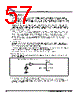
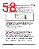
58 / 121 page 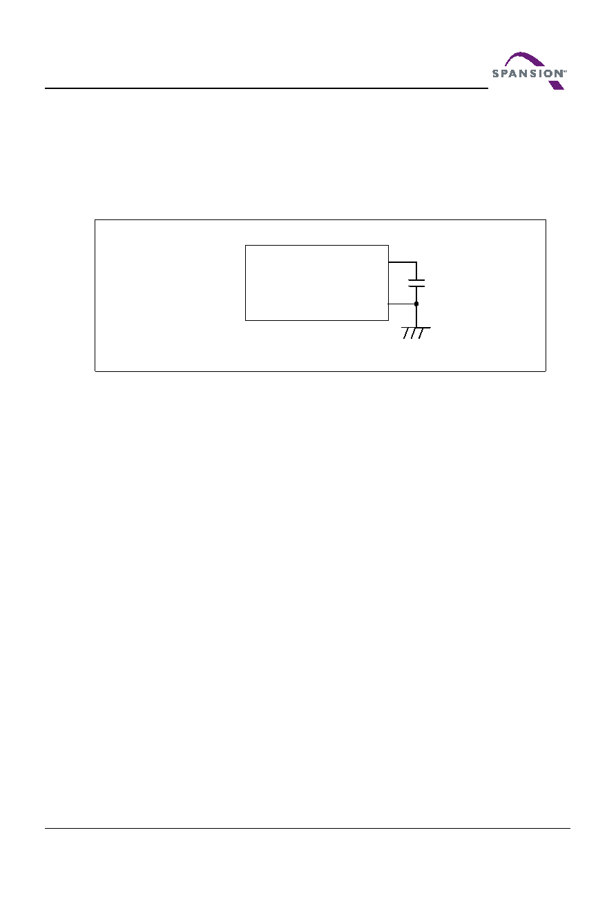 D a t a S h e e t March 11, 2015, MB9B410R-DS706-00026-3v0-E 55 CONFIDENTIAL C Pin This series contains the regulator. Be sure to connect a smoothing capacitor (CS) for the regulator between the C pin and the GND pin. Please use a ceramic capacitor or a capacitor of equivalent frequency characteristics as a smoothing capacitor. However, some laminated ceramic capacitors have the characteristics of capacitance variation due to thermal fluctuation (F characteristics and Y5V characteristics). Please select the capacitor that meets the specifications in the operating conditions to use by evaluating the temperature characteristics of a capacitor. A smoothing capacitor of about 4.7μF would be recommended for this series. Mode pins (MD0) Connect the MD pin (MD0) directly to VCC or VSS pins. Design the printed circuit board such that the pull-up/down resistance stays low, as well as the distance between the mode pins and VCC pins or VSS pins is as short as possible and the connection impedance is low, when the pins are pulled-up/down such as for switching the pin level and rewriting the Flash memory data. It is because of preventing the device erroneously switching to test mode due to noise. Notes on power-on Turn power on/off in the following order or at the same time. If not using the A/D converter, connect AVCC = VCC and AVSS = VSS. Turning on : VCC → AVCC → AVRH Turning off : AVRH → AVCC → VCC Serial Communication There is a possibility to receive wrong data due to the noise or other causes on the serial communication. Therefore, design a printed circuit board so as to avoid noise. Consider the case of receiving wrong data due to noise, perform error detection such as by applying a checksum of data at the end. If an error is detected, retransmit the data. Differences in features among the products with different memory sizes and between Flash products and MASK products The electric characteristics including power consumption, ESD, latch-up, noise characteristics, and oscillation characteristics among the products with different memory sizes and between Flash products and MASK products are different because chip layout and memory structures are different. If you are switching to use a different product of the same series, please make sure to evaluate the electric characteristics. Pull-Up function of 5 V tolerant I/O Please do not input the signal more than VCC voltage at the time of Pull-Up function use of 5 V tolerant I/O. Device C VSS CS GND |
|
Link URL |
| Does ALLDATASHEET help your business so far? [ DONATE ] |
About Alldatasheet | Advertisement | Contact us | Privacy Policy | Link to Datasheet | Link Exchange | Manufacturer List All Rights Reserved©Alldatasheet.com |
| Russian : Alldatasheetru.com | Korean : Alldatasheet.co.kr | Spanish : Alldatasheet.es | French : Alldatasheet.fr | Italian : Alldatasheetit.com Portuguese : Alldatasheetpt.com | Polish : Alldatasheet.pl | Vietnamese : Alldatasheet.vn Indian : Alldatasheet.in | Mexican : Alldatasheet.com.mx | British : Alldatasheet.co.uk | New Zealand : Alldatasheet.co.nz |
|
Family Site : ic2ic.com |
icmetro.com |
 British ▼
 English
 Chinese
 German
 Japanese
 Russian
 Korean
 Spanish
 French
 Italian
 Portuguese
 Polish
 Vietnamese
 Indian
 Mexican
 British
 New Zealand