|
Electronic Components Datasheet Search |
|
|
Electronic Components Datasheet Search |
|
ADDR10 Datasheet(PDF) 14 Page - List of Unclassifed Manufacturers |
|
|
|||||||||||||||||||||||||||||
ADDR10 Datasheet(HTML) 14 Page - List of Unclassifed Manufacturers |
|
|
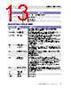
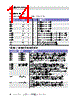
14 / 68 page 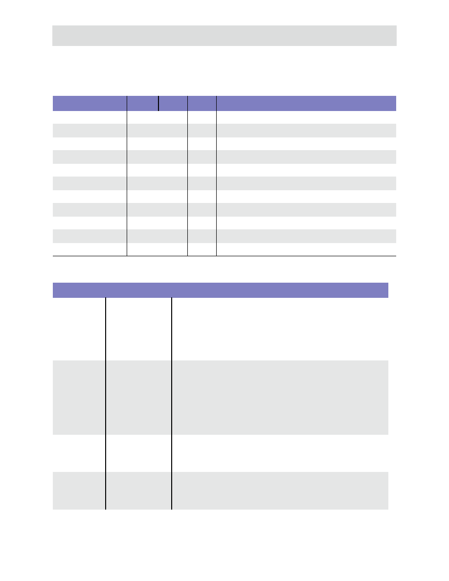 C h i p selec t co ntro ller 10 NS 75 20 Da ta shee t 03 /2 00 6 Chip select controller The NS7520 supports five unique chip select configurations. Chip select controller signal descriptions Symbol Pin I/O OD Description CS4_ B4 O 4 Chip select/DRAM RAS_ CS3_ A4 O 4 Chip select/DRAM RAS_ CS2_ C5 O 4 Chip select/DRAM RAS_ CS1_ B5 O 4 Chip select/DRAM RAS_ CS0_ D5 O 4 Chip select (boot select) CAS3_ A1 O 4 FP/EDO DRAM column strobe D31:D24/SDRAM RAS_ CAS2_ C4 O 4 FP/EDO DRAM column strobe D23:D16/SDRAM CAS_ CAS1_ B3 O 4 FP/EDO DRAM column strobe D15:D08/SDRAM WE_ CAS0_ A2 O 4 FP/EDO DRAM column strobe D07:D00/SDRAM A10(AP) WE_ C6 O 4 Write enable for NCC Ctrl’d cycles OE_ B6 O 4 Output enable for NCC Ctrl’d cycles Mnemonic Signal Description CS0_ CS1_ CS2_ CS3_ CS4_ Chip select 0 Chip select 1 Chip select 2 Chip select 3 Chip select 4 Unique chip select outputs supported by the NS7520. Each chip select can be configured to decode a portion of the available address space and can address a maximum of 256 Mbytes of address space. The chip selects are configured using registers in the memory module. A chip select signal is driven low to indicate the end of the current memory cycle. For FP/EDO DRAM, these signals provide the RAS signal. CAS0_ CAS1_ CAS2_ CAS3_ Column address strobe signals Activated when an address is decoded by a chip select module configured for DRAM mode. The CAS_ signals are active low and provide the column address strobe function for DRAM devices. The CAS_ signals also identify which 8-bit bytes of the 32-bit data bus are active during any given system bus memory cycle. For SDRAM, CAS[3:1]_ provides the SDRAM command field. CAS0_ provides the auto-precharge signal. For non-DRAM settings, these signals are 1. WE_ Write enable Active low signal that indicates that a memory write cycle is in progress. This signal is activated only during write cycles to peripherals controlled by one of the chip selects in the memory module. OE_ Output enable Active low signal that indicates that a memory read cycle is in progress. This signal is activated only during read cycles from peripherals controlled by one of the chip selects in the memory module. |
|
Link URL |
| Does ALLDATASHEET help your business so far? [ DONATE ] |
About Alldatasheet | Advertisement | Contact us | Privacy Policy | Link to Datasheet | Link Exchange | Manufacturer List All Rights Reserved©Alldatasheet.com |
| Russian : Alldatasheetru.com | Korean : Alldatasheet.co.kr | Spanish : Alldatasheet.es | French : Alldatasheet.fr | Italian : Alldatasheetit.com Portuguese : Alldatasheetpt.com | Polish : Alldatasheet.pl | Vietnamese : Alldatasheet.vn Indian : Alldatasheet.in | Mexican : Alldatasheet.com.mx | British : Alldatasheet.co.uk | New Zealand : Alldatasheet.co.nz |
|
Family Site : ic2ic.com |
icmetro.com |
 British ▼
 English
 Chinese
 German
 Japanese
 Russian
 Korean
 Spanish
 French
 Italian
 Portuguese
 Polish
 Vietnamese
 Indian
 Mexican
 British
 New Zealand