|
Electronic Components Datasheet Search |
|
|
Electronic Components Datasheet Search |
|
ADDR10 Datasheet(PDF) 7 Page - List of Unclassifed Manufacturers |
|
|
|||||||||||||||||||||||||||||
ADDR10 Datasheet(HTML) 7 Page - List of Unclassifed Manufacturers |
|
|
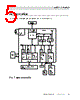
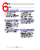
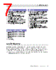
7 / 68 page  Operating freque ncy ww w.d i gi .c om 3 Operating frequency The NS7520 is available in grades operating at three maximum operating frequencies: 36 MHz, 46 MHz, and 55 MHz. The operating frequency is set during bootstrap initialization, using pins A[8:0]. These address pins load the PLL Settings register on powerup reset. A[8:7] determines IS (charge pump current); A[6:5] determines FS (output divider), and A[4:0] defines ND (PLL multiplier). Each bit in A[8:0] can be set individually. See the discussion of the PLL Settings register in the NS7520 Hardware Reference for more information. Serial ports Bus interface Two fully independent serial ports (UART, SPI) Digital phase lock loop (DPLL) for receive clock extractions 32-byte transmit/receive FIFOs Internal programmable bit-rate generators Bit rates 75–230400 in 16X mode Bit rates 1200 bps–4 Mbps in 1X mode Flexible baud rate generator, external clock for synchronous operation Receive-side character and buffer gap timers Four receive-side data match detectors Five independent programmable chip selects with 256 Mb addressing per chip select Chip select support for SRAM, FP/EDO DRAM, SDRAM, Flash, and EEPROM without external glue 8-, 16-, and 32-bit peripheral support External address decoding and cycle termination Dynamic bus sizing Internal DRAM/SDRAM controller with address multiplexer and programmable refresh frequency Internal refresh controller (CAS before RAS) Burst-mode support 0–63 wait states per chip select Address pins that configurem chip operating modes (see "NS7520 bootstrap initialization" on page 22) Power and Operating Voltages 500 mW maximum at 55 MHz (all outputs switching) 418 mW maximum at 46 MHz (all outputs switching) 291 mW maximum at 36 MHz (all outputs switching) 3.3 V — I/O 1.5 V — Core |
|
Link URL |
| Does ALLDATASHEET help your business so far? [ DONATE ] |
About Alldatasheet | Advertisement | Contact us | Privacy Policy | Link to Datasheet | Link Exchange | Manufacturer List All Rights Reserved©Alldatasheet.com |
| Russian : Alldatasheetru.com | Korean : Alldatasheet.co.kr | Spanish : Alldatasheet.es | French : Alldatasheet.fr | Italian : Alldatasheetit.com Portuguese : Alldatasheetpt.com | Polish : Alldatasheet.pl | Vietnamese : Alldatasheet.vn Indian : Alldatasheet.in | Mexican : Alldatasheet.com.mx | British : Alldatasheet.co.uk | New Zealand : Alldatasheet.co.nz |
|
Family Site : ic2ic.com |
icmetro.com |
 British ▼
 English
 Chinese
 German
 Japanese
 Russian
 Korean
 Spanish
 French
 Italian
 Portuguese
 Polish
 Vietnamese
 Indian
 Mexican
 British
 New Zealand