|
Electronic Components Datasheet Search |
|
|
Electronic Components Datasheet Search |
|
ADDR10 Datasheet(PDF) 50 Page - List of Unclassifed Manufacturers |
|
|
|||||||||||||||||||||||||||||
ADDR10 Datasheet(HTML) 50 Page - List of Unclassifed Manufacturers |
|
|
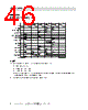
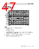
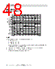
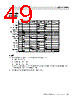
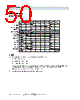
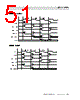
50 / 68 page 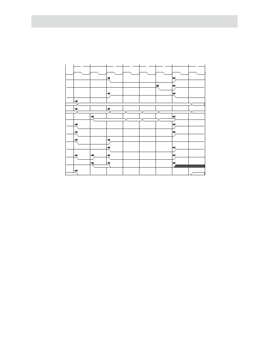 SDR A M ti ming 46 NS 93 60 Da ta shee t 03 /2 00 6 SDRAM burst write SDRAM burst write Notes: 1 Port size determines which byte enable signals are active: – 8-bit port = BE3* – 16-bit port = BE[3:2] – 32-bit port = BE[3:0] 2 The precharge and/or active commands are not always present. These commands depend on the address of the previous SDRAM access. When the active command is not present, parameter #35 is valid during the write (T2) cycle. 3 The TA* and TEA*/LAST signals are for reference only. T1 T2 T2 T2 T2 T1 prechg active write write write write inhibit 12 34 34 34 34 34 34 34 34 34 34 34 27 27 36 36 13 9 35 35 6 37 37 31 31 30 30 A10 BCLK TA* (Note-3) TEA*/LAST* (Note-3) PortA2/AMUX Non-muxed address Muxed address write D[31:0]1 BE[3:0]* (DQM) CS[4:0]* CAS3* (RAS) CAS2* (CAS) CAS1* (WE) CAS0* (A10/AP) RW* |
|
Link URL |
| Does ALLDATASHEET help your business so far? [ DONATE ] |
About Alldatasheet | Advertisement | Contact us | Privacy Policy | Link to Datasheet | Link Exchange | Manufacturer List All Rights Reserved©Alldatasheet.com |
| Russian : Alldatasheetru.com | Korean : Alldatasheet.co.kr | Spanish : Alldatasheet.es | French : Alldatasheet.fr | Italian : Alldatasheetit.com Portuguese : Alldatasheetpt.com | Polish : Alldatasheet.pl | Vietnamese : Alldatasheet.vn Indian : Alldatasheet.in | Mexican : Alldatasheet.com.mx | British : Alldatasheet.co.uk | New Zealand : Alldatasheet.co.nz |
|
Family Site : ic2ic.com |
icmetro.com |
 British ▼
 English
 Chinese
 German
 Japanese
 Russian
 Korean
 Spanish
 French
 Italian
 Portuguese
 Polish
 Vietnamese
 Indian
 Mexican
 British
 New Zealand