|
Electronic Components Datasheet Search |
|
|
Electronic Components Datasheet Search |
|
MB9BF412RPMC-G-JNE2 Datasheet(PDF) 39 Page - Cypress Semiconductor |
|
|
|||||||||||||||||||||||||||||
MB9BF412RPMC-G-JNE2 Datasheet(HTML) 39 Page - Cypress Semiconductor |
|
|
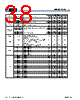
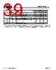
39 / 112 page 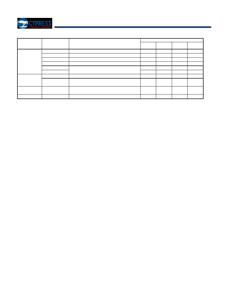 Document Number: 002-05615 Rev. *D Page 39 of 112 MB9B410R Series Module Pin name Function Pin No LQFP- 100 FBGA- 112 LQFP- 120 QFP- 100 Clock X0 Main clock (oscillation) input pin 48 L9 58 26 X0A Sub clock (oscillation) input pin 36 L3 41 14 X1 Main clock (oscillation) I/O pin 49 L10 59 27 X1A Sub clock (oscillation) I/O pin 37 K3 42 15 CROUT_0 Built-in high-speed CR-osc clock output port 74 C10 89 52 CROUT_1 92 B5 107 70 Analog Power AVCC A/D converter analog power pin 60 H11 70 38 AVRH A/D converter analog reference voltage input pin 61 F11 71 39 Analog GND AVSS A/D converter GND pin 62 G11 72 40 C pin C Power stabilization capacity pin 33 L2 38 11 Note: − While this device contains a Test Access Port (TAP) based on the IEEE 1149.1-2001 JTAG standard, it is not fully compliant to all requirements of that standard. This device may contain a 32-bit device ID that is the same as the 32-bit device ID in other devices with different functionality. The TAP pins may also be configurable for purposes other than access to the TAP controller. |
|
Link URL |
| Does ALLDATASHEET help your business so far? [ DONATE ] |
About Alldatasheet | Advertisement | Contact us | Privacy Policy | Link to Datasheet | Link Exchange | Manufacturer List All Rights Reserved©Alldatasheet.com |
| Russian : Alldatasheetru.com | Korean : Alldatasheet.co.kr | Spanish : Alldatasheet.es | French : Alldatasheet.fr | Italian : Alldatasheetit.com Portuguese : Alldatasheetpt.com | Polish : Alldatasheet.pl | Vietnamese : Alldatasheet.vn Indian : Alldatasheet.in | Mexican : Alldatasheet.com.mx | British : Alldatasheet.co.uk | New Zealand : Alldatasheet.co.nz |
|
Family Site : ic2ic.com |
icmetro.com |
 British ▼
 English
 Chinese
 German
 Japanese
 Russian
 Korean
 Spanish
 French
 Italian
 Portuguese
 Polish
 Vietnamese
 Indian
 Mexican
 British
 New Zealand