|
Electronic Components Datasheet Search |
|
|
Electronic Components Datasheet Search |
|
MB9BF412RPMC-G-JNE2 Datasheet(PDF) 1 Page - Cypress Semiconductor |
|
|
|||||||||||||||||||||||||||||
MB9BF412RPMC-G-JNE2 Datasheet(HTML) 1 Page - Cypress Semiconductor |
|
|
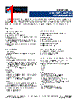
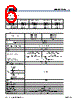
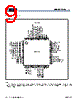
1 / 112 page  MB9B410R Series 32-bit Arm® Cortex®-M3 FM3 Microcontroller Cypress Semiconductor Corporation • 198 Champion Court • San Jose , CA 95134-1709 Document Number: 002-05615 Rev. *D • 408-943-2600 Revised February 9, 2018 The MB9B410R Series are highly integrated 32-bit microcontrollers dedicated for embedded controllers with high-performance and competitive cost. These series are based on the Arm Cortex-M3 Processor with on-chip Flash memory and SRAM, and has peripheral functions such as Motor Control Timers, ADCs and Communication Interfaces (CAN, UART, CSIO, I2C, LIN). The products which are described in this data sheet are placed into TYPE4 product categories in FM3 Family Peripheral Manual. Features 32-bit Arm Cortex-M3 Core Processor version: r2p1 Up to 144MHz Frequency Operation Memory Protection Unit (MPU): improves the reliability of an embedded system Integrated Nested Vectored Interrupt Controller (NVIC): 1 NMI (non-maskable interrupt) and 48 peripheral interrupts and 16 priority levels 24-bit System timer (Sys Tick): System timer for OS task management On-chip Memories [Flash memory] These series are based on two independent on-chip Flash memories. MainFlash Up to 512 Kbyte Built-in Flash Accelerator System with 16 Kbyte trace buffer memory The read access to Flash memory can be achieved without wait cycle up to operation frequency of 72 MHz. Even at the operation frequency more than 72 MHz, an equivalent access to Flash memory can be obtained by Flash Accelerator System. Security function for code protection WorkFlash 32 Kbyte Read cycle 4 wait-cycle: the operation frequency more than 72 MHz 2 wait-cycle: the operation frequency more than 40 MHz, and to 72 MHz 0 wait-cycle: the operation frequency to 40 MHz Security function is shared with code protection [SRAM] This Series contain a total of up to 64 Kbyte on-chip SRAM. This is composed of two independent SRAM (SRAM0, SRAM1). SRAM0 is connected to I-code bus and D-code bus of Cortex-M3 core. SRAM1 is connected to System bus. SRAM0: Up to 32 Kbyte SRAM1: Up to 32 Kbyte External Bus Interface Supports SRAM, NOR and NAND Flash device Up to 8 chip selects 8-/16-bit Data width Up to 25-bit Address bit Maximum area size: Up to 256 Mbytes Supports Address/Data multiplex Supports external RDY input CAN Interface (Max two channels) Compatible with CAN Specification 2.0A/B Maximum transfer rate: 1 Mbps Built-in 32 message buffer Multi-function Serial Interface (Max eight channels) 4 channels with 16 steps×9-bit FIFO (ch.4 to ch.7), 4 channels without FIFO (ch.0 to ch.3) Operation mode is selectable from the followings for each channel. UART CSIO LIN I2C UART Full-duplex double buffer Selection with or without parity supported Built-in dedicated baud rate generator External clock available as a serial clock Hardware Flow control: Automatically control the transmission by CTS/RTS (only ch.4) Various error detect functions available (parity errors, framing errors, and overrun errors) CSIO Full-duplex double buffer Built-in dedicated baud rate generator Overrun error detect function available |
Similar Part No. - MB9BF412RPMC-G-JNE2 |
|
Similar Description - MB9BF412RPMC-G-JNE2 |
|
|
Link URL |
| Does ALLDATASHEET help your business so far? [ DONATE ] |
About Alldatasheet | Advertisement | Contact us | Privacy Policy | Link to Datasheet | Link Exchange | Manufacturer List All Rights Reserved©Alldatasheet.com |
| Russian : Alldatasheetru.com | Korean : Alldatasheet.co.kr | Spanish : Alldatasheet.es | French : Alldatasheet.fr | Italian : Alldatasheetit.com Portuguese : Alldatasheetpt.com | Polish : Alldatasheet.pl | Vietnamese : Alldatasheet.vn Indian : Alldatasheet.in | Mexican : Alldatasheet.com.mx | British : Alldatasheet.co.uk | New Zealand : Alldatasheet.co.nz |
|
Family Site : ic2ic.com |
icmetro.com |
 British ▼
 English
 Chinese
 German
 Japanese
 Russian
 Korean
 Spanish
 French
 Italian
 Portuguese
 Polish
 Vietnamese
 Indian
 Mexican
 British
 New Zealand