 |
Electronic Components Datasheet Search |
|
|
Electronic Components Datasheet Search |
|
MB96F348CWCPMC-GSE2 Datasheet(PDF) 14 Page - Cypress Semiconductor |
|
|
|||||||||||||||||||||||||||||
MB96F348CWCPMC-GSE2 Datasheet(HTML) 14 Page - Cypress Semiconductor |
|
|
14 / 109 page 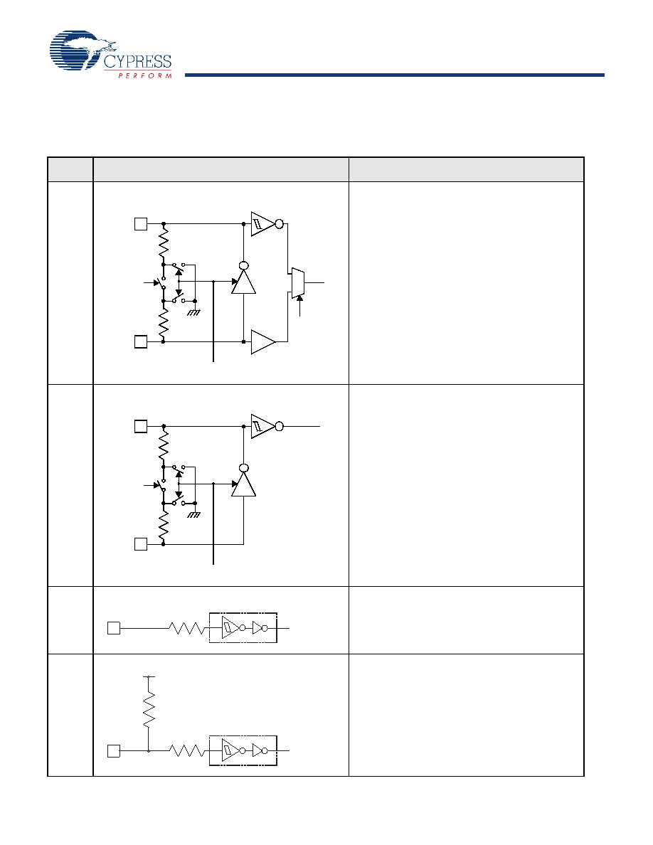 MB96340 Series Document Number: 002-04579 Rev. *A Page 14 of 109 6. I/O Circuit Type Type Circuit Remarks A High-speed oscillation circuit: ■ Programmable between oscillation mode (external crystal or resonator connected to X0/X1 pins) and Fast external Clock Input (FCI) mode (external clock connected to X0 pin) ■ Programmable feedback resistor = approx. 2 * 0.5 M. Feedback resistor is grounded in the center when the oscillator is disabled or in FCI mode B Low-speed oscillation circuit: ■ Programmable feedback resistor = approx. 2 * 5 M. Feedback resistor is grounded in the center when the oscillator is disabled C ■ Mask ROM and EVA device:CMOS Hysteresis input pin ■ Flash device:CMOS input pin E ■ CMOS Hysteresis input pin ■ Pull-up resistor value: approx. 50 k X1 X0 R R MRFBE Xout FCI 0 1 FCI or osc disable X1A X0A R R SRFBE Xout osc disable R Hysteresis inputs R Pull-up Resistor Hysteresis inputs |
|
Link URL |
| Does ALLDATASHEET help your business so far? [ DONATE ] |
About Alldatasheet | Advertisement | Contact us | Privacy Policy | Link to Datasheet | Link Exchange | Manufacturer List All Rights Reserved©Alldatasheet.com |
| Russian : Alldatasheetru.com | Korean : Alldatasheet.co.kr | Spanish : Alldatasheet.es | French : Alldatasheet.fr | Italian : Alldatasheetit.com Portuguese : Alldatasheetpt.com | Polish : Alldatasheet.pl | Vietnamese : Alldatasheet.vn Indian : Alldatasheet.in | Mexican : Alldatasheet.com.mx | British : Alldatasheet.co.uk | New Zealand : Alldatasheet.co.nz |
|
Family Site : ic2ic.com |
icmetro.com |
 British ▼
 English
 Chinese
 German
 Japanese
 Russian
 Korean
 Spanish
 French
 Italian
 Portuguese
 Polish
 Vietnamese
 Indian
 Mexican
 British
 New Zealand


